Table of Contents
1. Introduction
1.1. Project description
The main goal of this project is to allow a person to read several books in one place. The books can be read at home or on the move thanks to a battery. Moreover, the books can be easily changed thanks to the micro SD card formatted in FAT32 (compatible with all operating systems) which is in the product. Unlike other E-Readers on the market, my project cannot read Epub files. An Epub to text file converter was therefore created.
When not in use, the product can be turned into a data logger. It automatically takes measurements and stores them on the micro SD card. Its low power consumption allows it to take certain measurements (temperature, humidity, etc.) over long periods without having to interact with it.
Two major constraints had to be taken into account. The first and most important constraint concerns the management of the circuit’s consumption. As the project is powered by a battery, it is imperative to limit consumption so as not to have to recharge it too often. Indeed, when the user is on the move, it is not always possible to recharge the battery. The second constraint is the size of the device. Since it can be used anywhere, it must be easy to carry, in a bag for example.
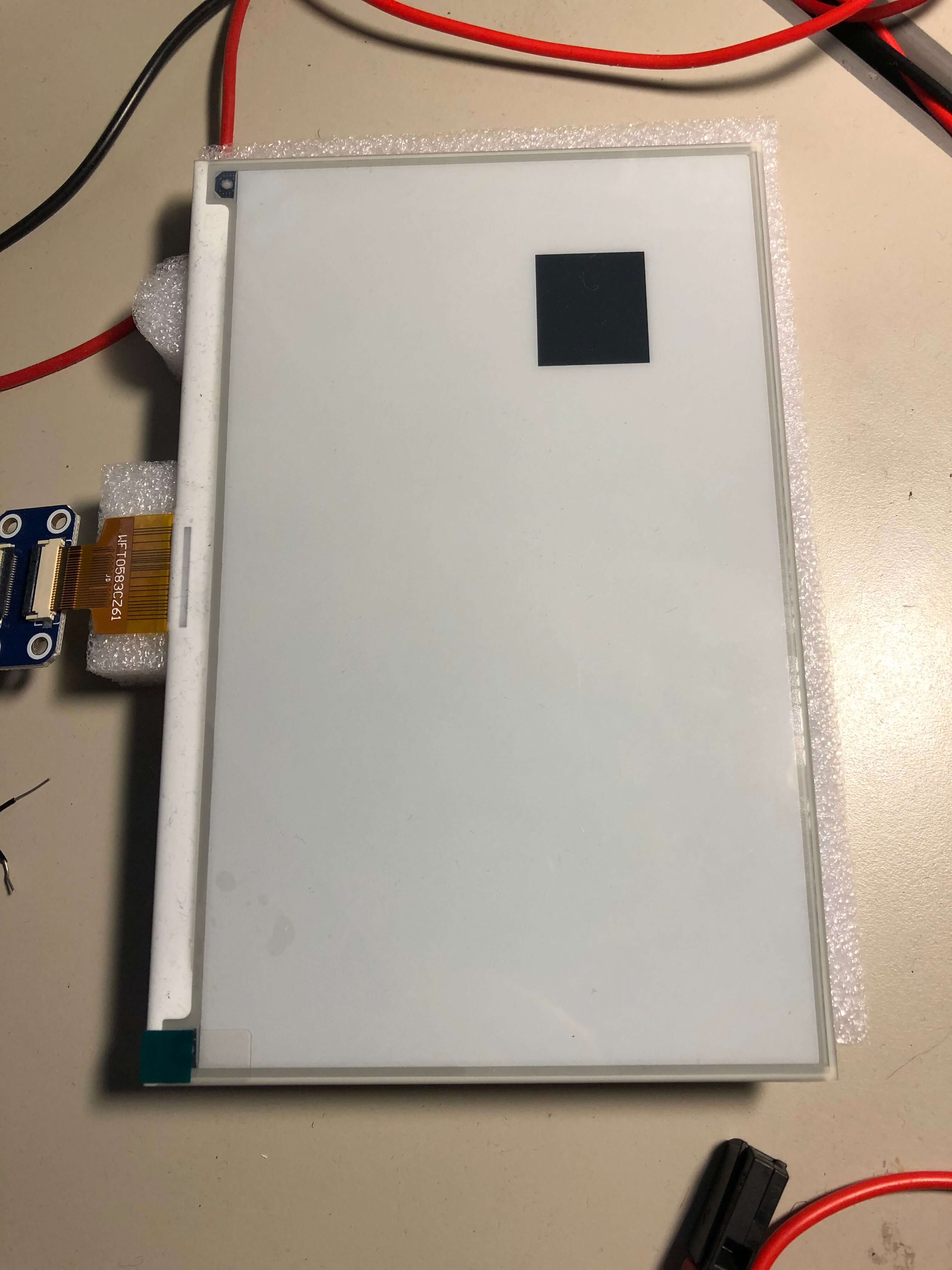
1.2. Photo of the finished product
2. Global analysis
2.1. Functional analysis
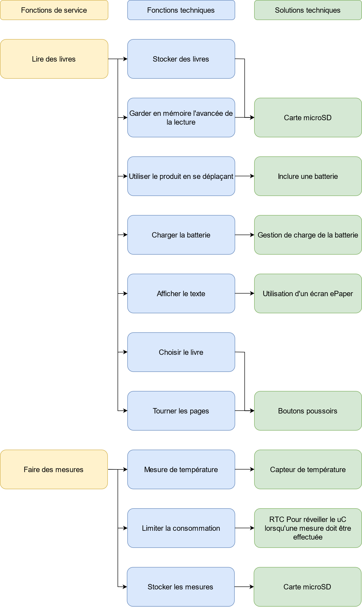
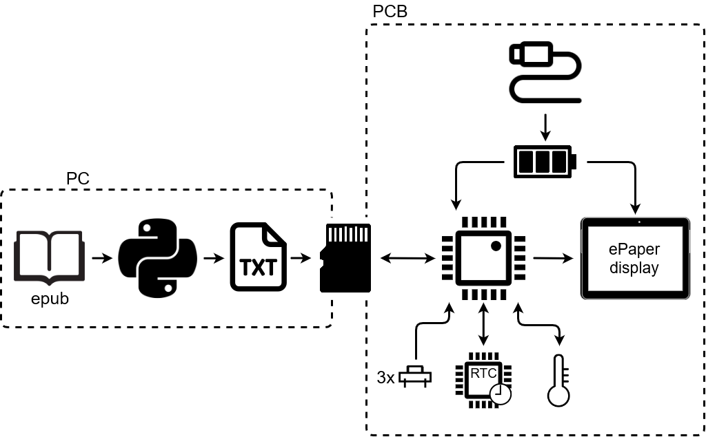
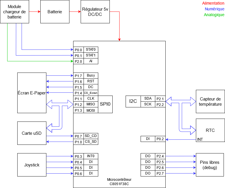
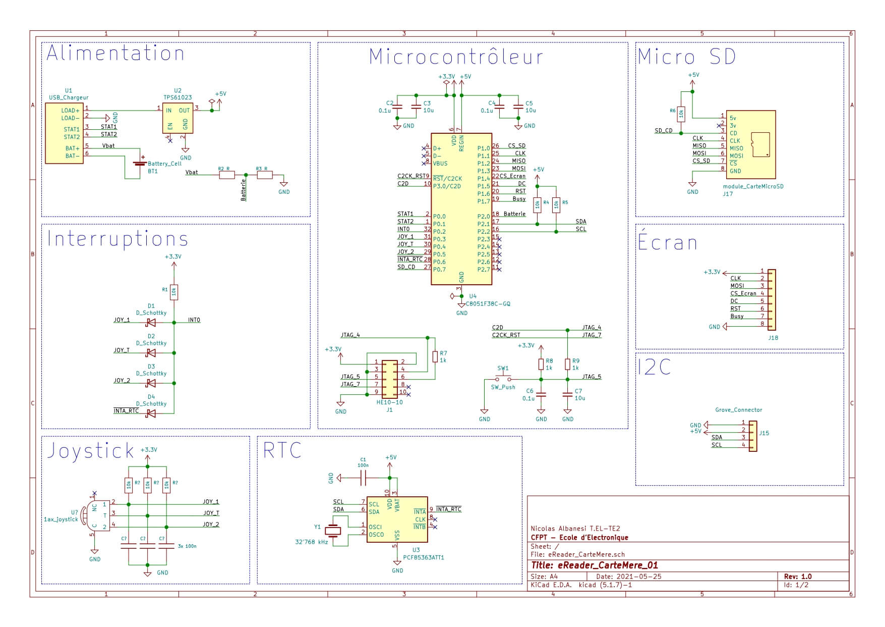
2.2. General block schematic
3. Bus description
3.1. SPI bus
3.1.1. Description
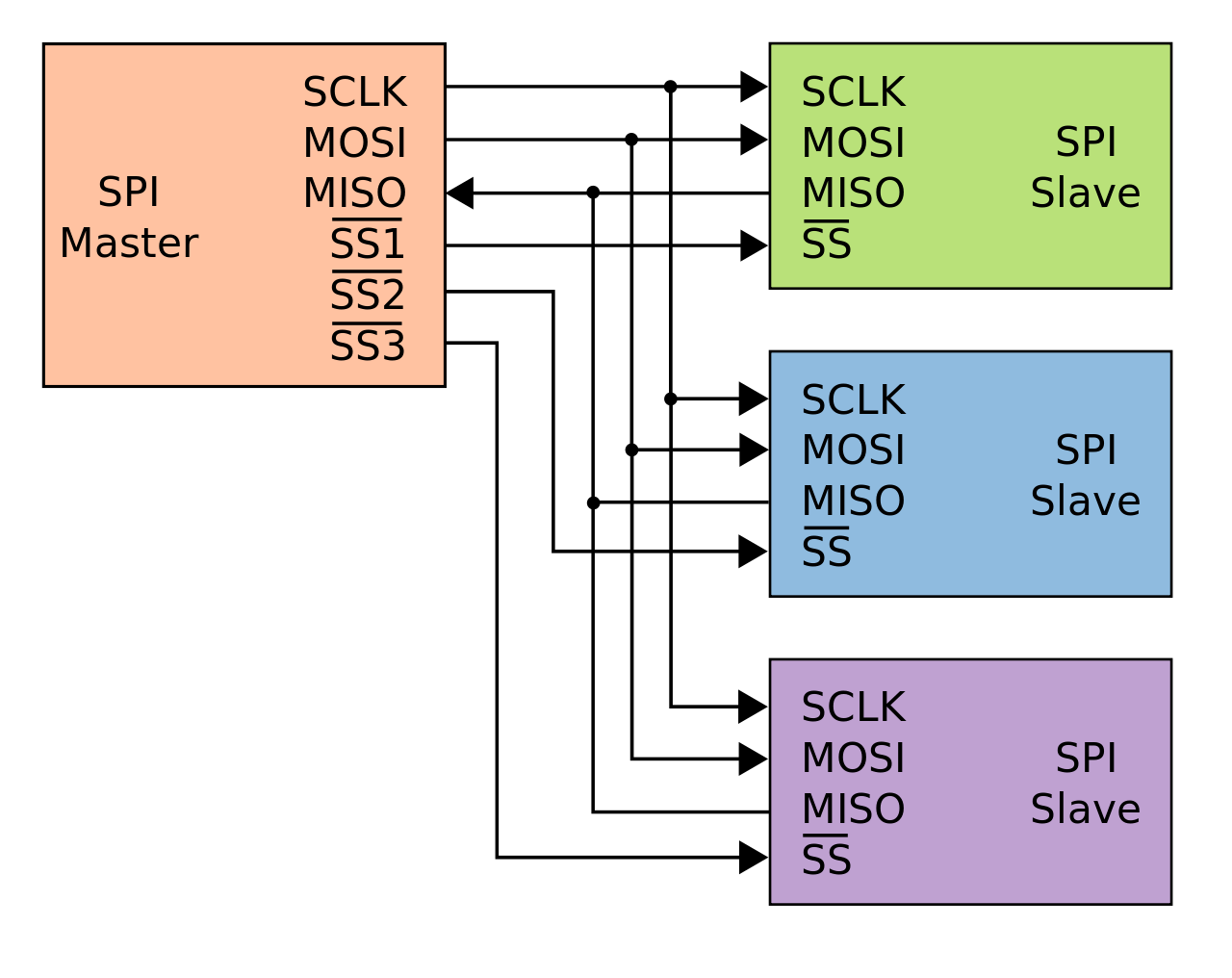
SPI (Serial Peripheral Interface) communication is a synchronous serial data bus (information is synchronised to a clock) in full-duplex mode (send and receive at the same time). Each link contains a master and at least one slave. However, several slaves can coexist on the same bus. The selection of the slave is done through a dedicated line called Slave Select (SS) or Chip Select (CS). Unlike I2C, there is no maximum number of slaves, the only limiting factor being the number of Slave Select lines.
The SPI bus uses a minimum of 4 logic signals when fully used. However, it is possible to use only 3 when the slave is not communicating back. For example, the display used during the project was only receiving information and not responding to the master, so the MISO line was not useful.
CLK |
Clock - Serial Clock (output from master) |
MOSI |
Master Out Slave In (data output from master) |
MISO |
Master In Slave Out (data output from slave) |
SS |
Slave Select - Select the slave chip |
The Example of an SPI connection shows an SPI connection with a master and 3 slaves. You can see that each slave has its own Slave Select line, and that they all share the CLK, MISO and MOSI lines.
3.1.2. Configuration
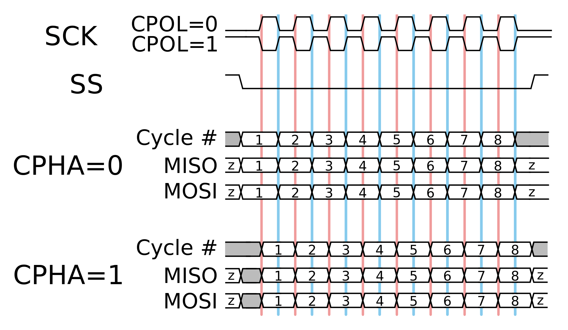
The SPI can be configured in 4 different modes. The chosen configuration depends on two bits: CPOL (Clock Polarity) and CPHA (Clock Phase). The CPOL bit configures the idle state of the CLK line, and the CPHA bit configures the edge on which the information is read (first or second). The timeline below shows the different configurations.
3.1.3. How it works
During communication, the master selects the slave it wants to communicate with by setting the Slave Select line to the logic low state. The master then generates a Clock, then at each edge (rising or falling, defined by CPHA) the master and slave transmit one bit to each other.
3.2. I2C Bus
3.2.1. Description
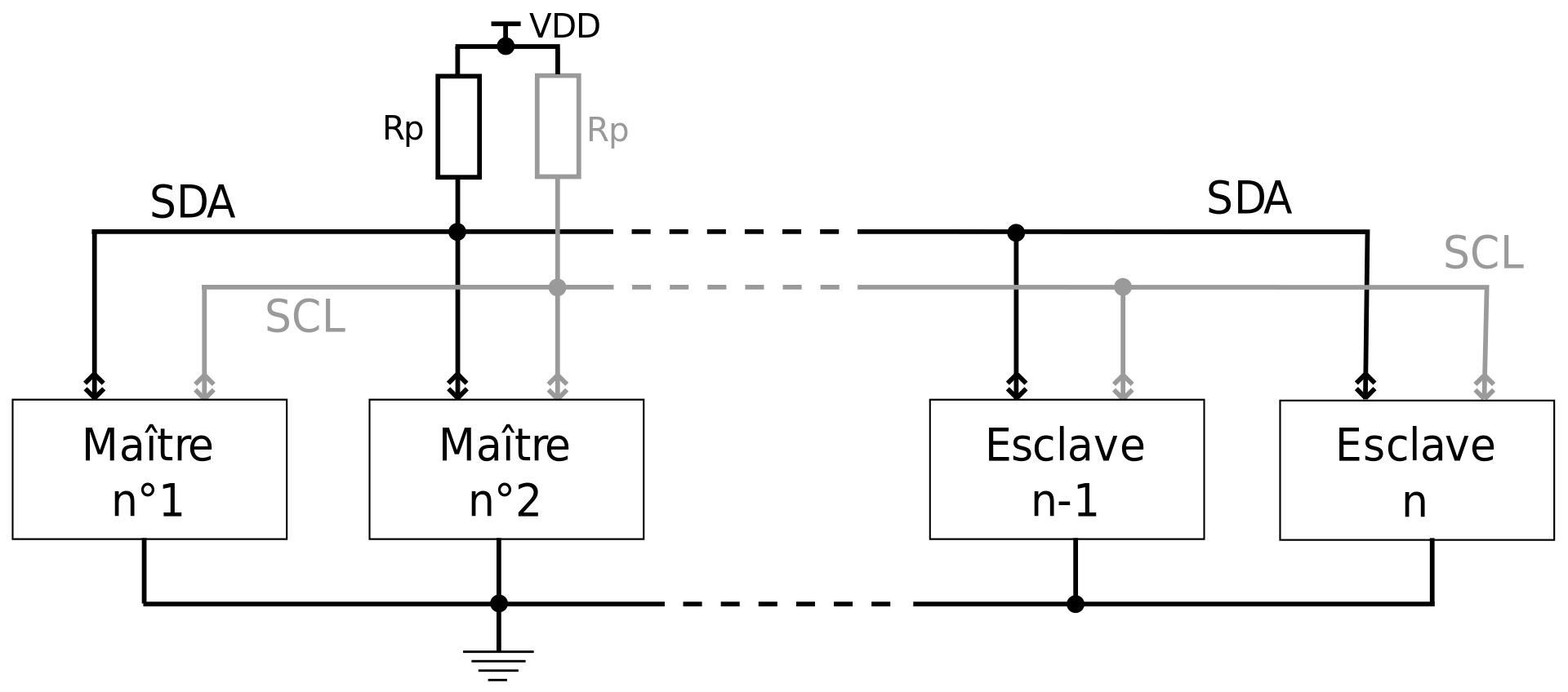
I2C (Inter-Integrated Circuit) communication is a synchronous (information is synchronised with a clock) half-duplex serial bus, i.e. the master can send information or receive it, but not both at the same time. Several masters and slaves can be connected to the bus at the same time. To address a slave, the master must start each message with the slave’s address. The addresses are coded on 7 bits, which limits the number of devices on a bus to 128. Some addresses are reserved for broadcast messages. As the addresses are fixed by the manufacturers, there may be two devices with the same address, which may affect their operation.
Exchanges are always from master to slave, never master-master or slave-slave. However, a master can become a slave and a slave can become a master at any time.
The advantage of the I2C bus is its reduced number of wires. To operate, the bus requires only 2 lines (SDA and SCL).
SDA |
Serial Data Line - Data Line |
SCL |
Serial Clock Line - Synchronisation clock line |
The Connection of peripherals on the I2C bus shows how to connect devices on the I2C bus.
Important
Do not forget to add pull-up resistors. Also, all grounds must be common.
3.2.2. How it works
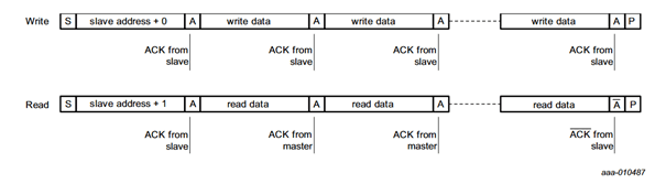
The diagram above shows the read and write protocol for an RTC (PCF85363A). Each frame starts with a START condition and then the slave address. Once the slave responds, we can then read or write information. To finalise the frame, a STOP condition is sent.
4. Conception and development
4.1. Epub file converter
The epub or “electronic publication” format is a standardised open format for digital books. It is based on XML and is not readable in a text editor. I don’t think it is possible to implement an epub interpreter on our microcontroller, and even less with the limited time of the project. So I chose to make an epub to text file converter, which can be read much more easily with the microcontroller.
This converter provides an advantage that is not negligible. By formatting the file, I can customize the formatting to make it easier to display later by specifying a certain number of characters per line. A disadvantage of the program is that it has no user interface, and must be run from a terminal.
The program runs in the following order :
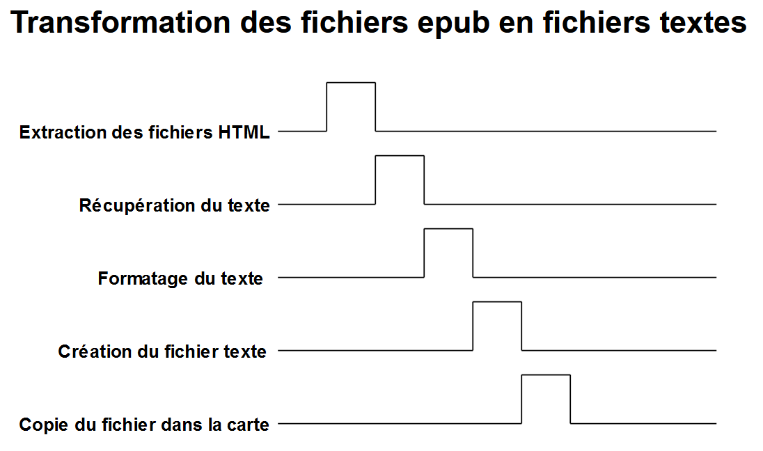
It is possible to view the contents of an epub file by renaming it to a zip file and then extracting its contents. The book consists of html files. Retrieving these files is the first action of the program. It will then extract the text from these html files using the html2text library. Once the text is retrieved, it is formatted using the justifytext library.
When the text file is created, a header is added, which makes it possible to keep in memory where the reader is in its reading. The Magic Number is used as a signature, when the microcontroller lists the available files, it displays only the files which have this signature.

Example usage :
> python main.py HPHBP.epub 40
Extracting Files...             Done
Filtering Files...              Done
Extracting Text...              Done
Formating Text...               Done
Deleting Files...               Done
The program need 2 parameters : the name of the epub file, and the number of characters per line
The Convertion result, shows that the file has been correctly converted. The first line is not displayed correctly because the application used shows the header added by the converter.
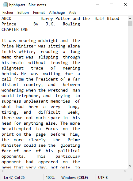
In the current version of the project, the converted text is raw. There’s only one size, and the titles are displayed in plain text.
4.2. MicroSD card
4.2.1. SD card classification
It is possible to classify SD cards in two categories. The capacity range and the writing speed. In both cases a logo is usually displayed on the card. The Comparison of SD card capacity standards compares the different sizes and displays the logo that can be found on the card.
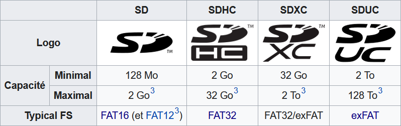
SDSC |
Secure Digital Standard Capactiy |
SDHC |
Secure Digital High Capacity |
SDXC |
Secure Digital eXtended Capacity |
SDUC |
Secure Digital Ultra Capacity |
The Typical FS line indicates the most suitable file system for each card. However, an SD card of 2GB or less can still be formatted in FAT32. A card larger than 2GB has no interest in being formatted in FAT12 or FAT16, as these file systems do not allow partitions larger than 2GB.
There is a difference between the SD card and SDHC, SDXC, and SDUC cards. The SD card is addressed in bytes, i.e. to read sector 0, the address is 0 and to read sector 1, the address is 512 (512 bytes per sector). SDHC, SDXC and SDUC cards are addressed by sectors. So to read sector 0, the address is 0 and to read sector 1, the address is 1.
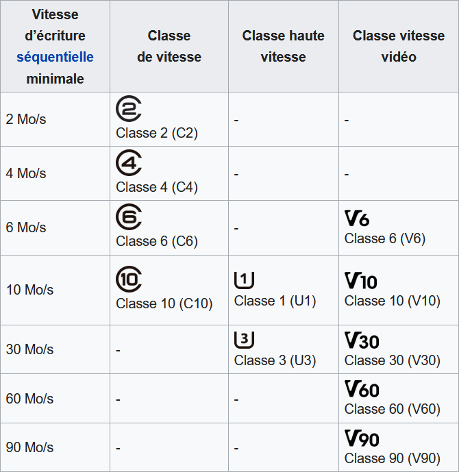
As said before, SD cards can also be classified according to their writing speed. The SD card minimal writing speed standards displays the different speeds along with their logo.
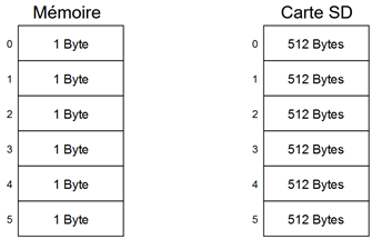
4.2.2. Comparison with a conventional memory
Like every memory, the SD card has addresses. At each address there is a sector (memory slot) of usually 512 bytes. A memory has, for example, a 1 byte memory cells. The communication is done in SPI, like some memories. In general, it is not possible to write a single bit in the memory, the whole byte must be written again. The SD card works in the same way. For example, it is not possible to write a single byte to address 0, you have to write 512 bytes at once. Similarly for reading, 512 bytes must be read at once.
4.2.3. Communication
To communicate with the card, there are two possible protocols: SD or SPI. The SD protocol is completely unknown to me, whereas SPI has already been used many times, so I chose it.
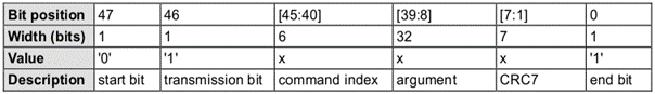
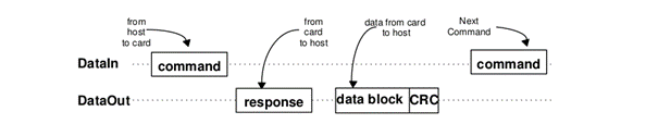
The communication is done via 48-bits long commands. The first byte contains the start bit, the transmit bit and the 6-bit command index. The next 4 bytes are the command argument and the last byte contains the CRC and the stop bit.
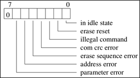
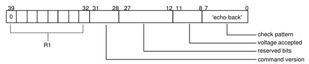
Once the command is received, the SD card sends a response. The most common response is the R1 response, there are also R2, R3 and R7 responses. Only the R1 and R7 responses were used during this project.
The R1 response tells us the status of the card and any errors in the command that has just been sent.
The response R7 is received after sending command 8, which is used during the card initialisation. It is used to set the board’s supply voltage. The command also has a check pattern which will be returned in the R7 response.
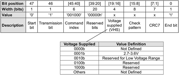
The R7 response has a size of 5 bytes. The first byte contains the same information as the R1 response and the next 4 bytes are specific to command 8.
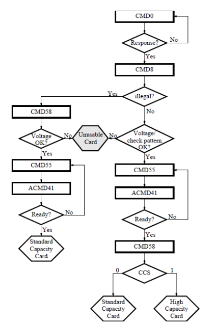
4.2.4. Initialisation
The first thing to do before the card can be used is to initialize it. The card must receive a sequence of commands that will prepare the card. If the list is completed, the type of card can be known.
4.2.5. Writing
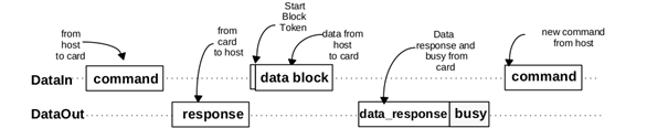
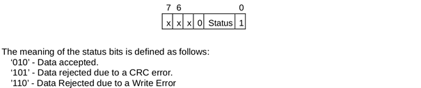
Once initialized, the card is ready to be used as a memory. To write to the card, you must first send the command 24 (WRITE_BLOCK) giving the address of the sector to write to as an argument. The card responds with the R1 response. If there is no problem, we need to send a start token (usually 0xFE) followed by the 512 bytes to be written. Once all the data has been sent, the card sends a response to indicate whether the data received was accepted or if there was an error (see data response format). The card then goes into busy mode while it writes all the received data into its memory.
4.2.6. Reading
Reading works like writing. You have to send the command 17 (READ_SINGLE_BLOCK) with the number of the sector to be read as argument. The card then responds with the R1 response to indicate any errors in the command. If there are no errors, the microcontroller will not send the token but will wait to receive it. Once the token is received, the next 512 bytes are the contents of the sector. The data will be followed by a 16-bit CRC.
4.2.7. Presence detection
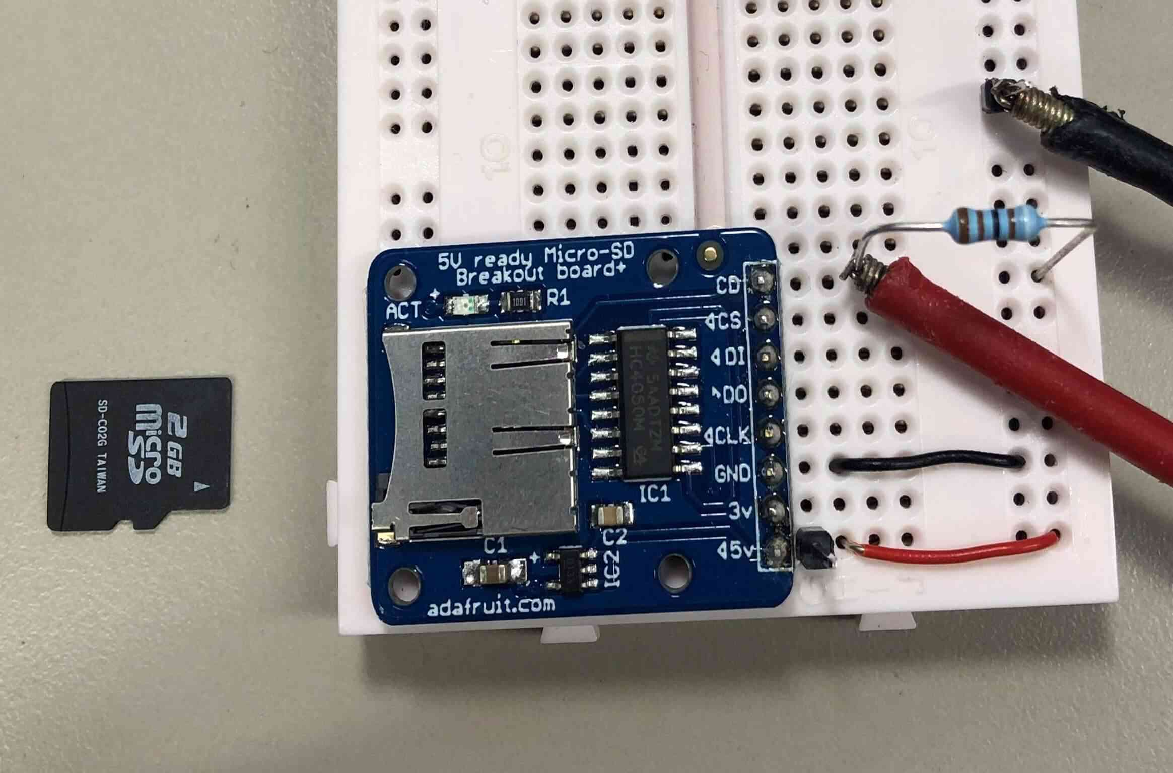
Since the micro SD card must be initialized before it can be used, it is necessary to ensure that the card is present before starting the initialization routine. Detecting the presence of the card will ensure that the card is not initialized without it being present. If the card is removed to add or remove books, it will need to be reset once reinserted.
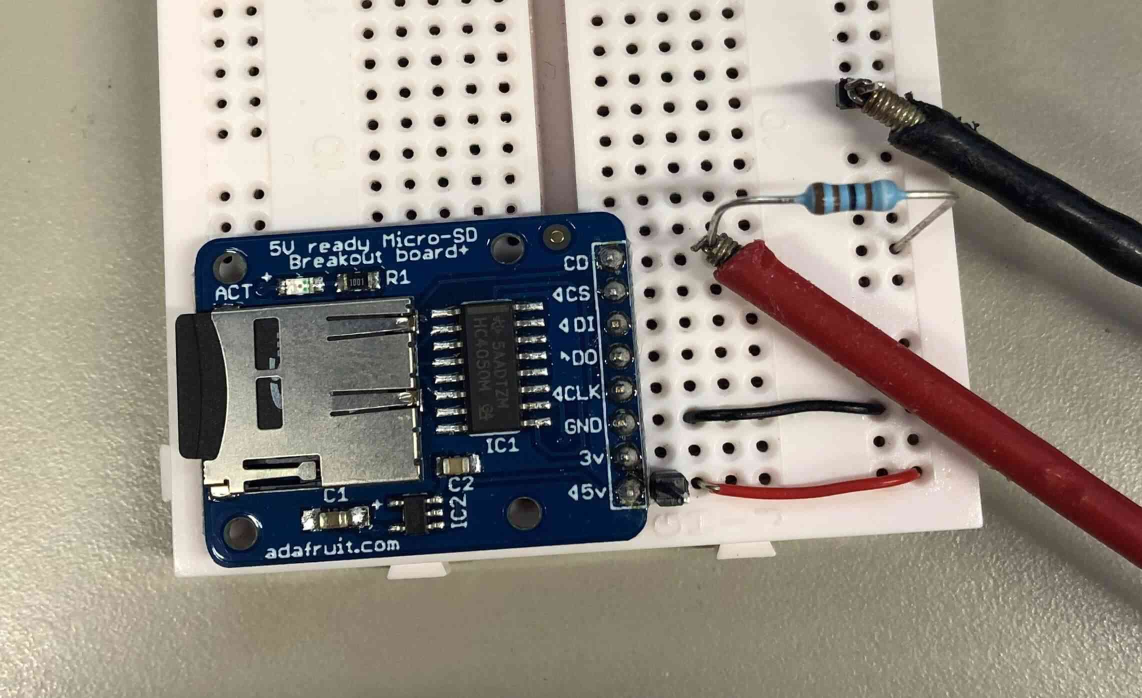
The micro SD card connector has a CD (Card Detect) pin. These indicate whether or not a card is inserted in the connector.
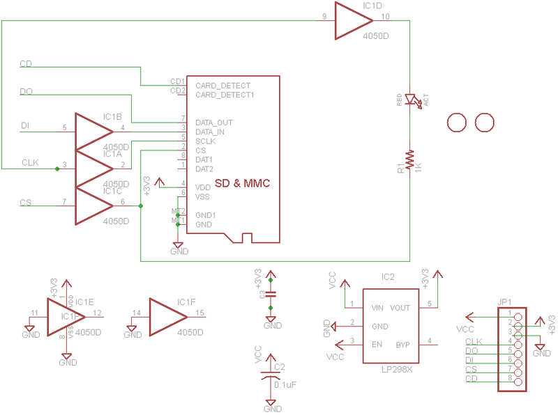
The CD pin is connected directly to the microcontroller, we just need to add a pull-up resistor. When a card is present in the connector, pin CD is at 5v. If no card is inserted, pin CD is pulled to ground, and the microcontroller reads a logic value of 0.
|
|
|
|
4.3. FAT32
FAT32 is a file system invented by Microsoft. A file system is used to organise files on a volume, in my case a micro SD card. It was important for me to understand FAT32 and to create a library with basic functions because for the user, the file transfer between the computer and the reader must be easy.
4.3.1. Regions
The volumes formatted in FAT32 are divided into 3 regions: the reserved region, the FAT region and the data region. The figure below shows the organisation of the regions on the micro SD card.
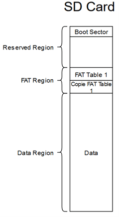
The first sector of the reserved region which is also the first sector of the SD card (Boot Sector) contains information allowing us to find the 2 other regions as well as information about these regions. We can also know the size of a cluster (explained later). In the FAT region, there is the FAT table and possibly copies of this table (indicated in the Boot Sector if there are any). The FAT table will be explained in more detail in the FAT Table section. Finally, the Data region contains the file entries as well as their contents.
Generally the first sector of the data region contains the root of the SD card in which we will find the file entries. A file entry always has a minimum size of 32 bytes. If the file name is larger than 8 characters, the size of the entry increases according to the size of the file name. Each file entry contains the following information:
-
Filename + extension
-
Attributs (hidden file, read-only, …)
-
Creation date of the file
-
Last modification date
-
File size (max 4 GB)
-
The cluster number of the file
4.3.2. Clusters
A cluster is a grouping of sectors. The number of sectors in the cluster is indicated in the BootSector. On Windows, when formatting, it is possible to choose how many sectors will be in a cluster.
|
|
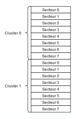
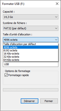
Since generally a sector is 512 Bytes, we know that if we choose 4096 Bytes, there will be 8 sectors per cluster (4096 / 512 = 8). It is important to know the size of a cluster because during the reading of a file, after having read a cluster, it is necessary to refer to the FAT table to find the next cluster.
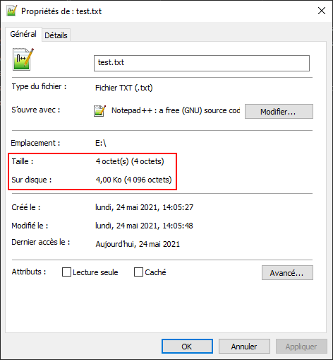
It is also important to know that when creating a file, a cluster is the minimum size of a file on the disk. That is, a text file that contains 4 characters should be 4 bytes in size. However, at least one cluster must be allocated per file, so the size will be 4096 bytes. This is observable when opening the properties of a file (see Size of a file on the disk)
4.3.3. FAT Table
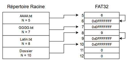
When reading a file, we must start by reading the first cluster of the file, then refer to the FAT table. This allows us to find the rest of the file on the volume if it continues or informs us that the file is finished. Each file has a Cluster Number which allows us to find the first cluster and which also allows us to find the right data in the FAT table. A simplified version of the FAT can be found below.
N stands for Cluster Number. For the file AAAA.txt, we can see that
its first number is 5. After reading the contents of the cluster we can
then go to the FAT table which tells us that the file continues with a
new number: 6. Once we have read this cluster we can go back to the
table and this time the table gives us the value 0x0FFFFFFF which
means the file does not continue.
In the case of the Simplified representation of the operation of the FAT table, the card has been
recently formatted and the numbers are consecutive. However the
principle of a file system is to find the content of a file even when it
is not consecutive. For example the file AAAA.txt could start with
number 5 and then continue with number 12.
4.3.4. Reading the BootSector
As mentioned before, the Boot Sector is the first sector of the card (address 0). It is important to read the information carefully, otherwise it will be impossible to find the other regions, and therefore the files.
Warning
The values are in Little Endian format, they must be changed to Big Endian format before doing the calculations
BPB_BytsPerSec |
Number of bytes per sector (512) |
BPB_SecPerClus |
Number of sector per cluster (8) |
BPB_RsvdSecCnt |
Number of sector in the reserved region (614) |
BPB_NumFATs |
Total number of FAT tables (2) |
BPB_FATSz32 |
Size of one FAT table (3789) |
BPB_RootClus |
Cluster number of the root directory (2) |
As we can see in the Organisation of the regions on a micro SD card, the FAT Table starts right after the reserved region. The size of the reserved region was read in the Boot Sector (BPB_RsvdSecCnt), it is 614 sectors. The FAT table starts at sector 614. There can be one or more copies of the FAT table (if BPB_NumFATs > 1). In our case there is one copy and it is located at sector 4403 (614 + 3789).
With this information we can also find the root directory. Since we know that it is located after the FAT region, we can find the first sector of the data region using the following formula:
RootDir = BPB_RsvdSecCnt + (BPB_NumFATs * FATSz32)
RootDir = 614 + (2 * 3789) = 8192
4.3.5. Reading the root directory
The root directory of the micro SD card is the highest level in the folder hierarchy. Since the root is a folder, the subfolders have exactly the same structure. The first entry contains the name of the SD card, it is not a file on the card.
Each file entry is 32 bytes, except for files with a name longer than 8 characters: The 32 byte base remains the same but there is in addition the full file name above the file entry (the long file name part has not really been explored).
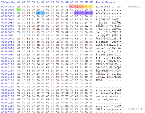
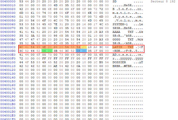
The red outlined part in the Root directory visualisation corresponds to the entry for a file named “latin.txt”. The first 11 bytes (in orange) corresponds to the file name, 8 bytes for the name and 3 for the extension. The next byte contains the file attributes.
We have seen in the Simplified representation of the operation of the FAT table, that each file has a cluster number. The two bytes in green are the 2 most significant bytes and the two bytes in blue are the least significant. In this case, the cluster number of the file is: 00 00 00 08 (do not forget to convert to Big Endian). The rest of the bytes contains the date and time of creation and the last modification as well as the size of the file.
Note
If the first byte of the file name is 0xE5, the file has been deleted and a new entry can be written to that location. If the value of the first byte is 0x00, all entries in the folder have been read.
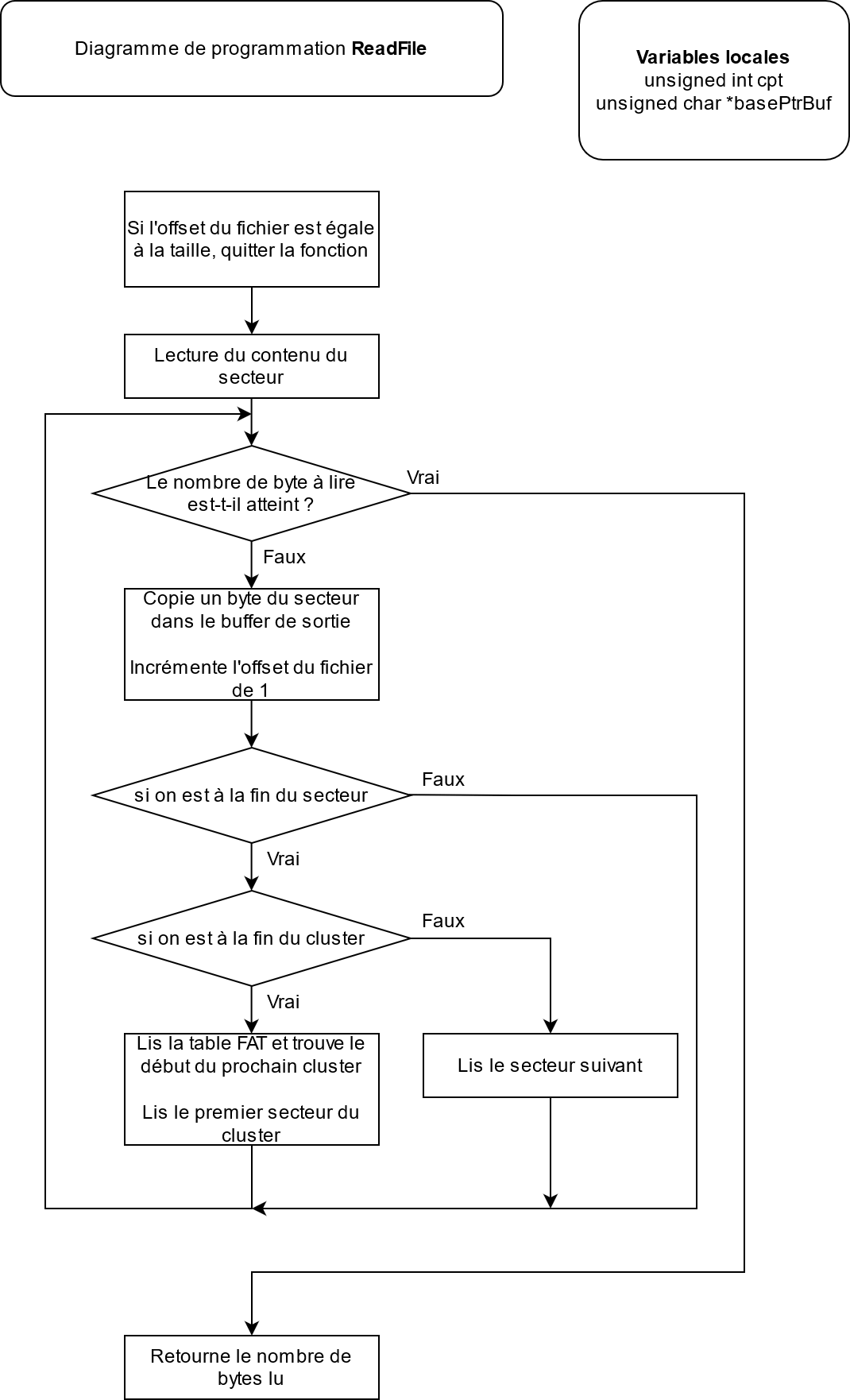
4.3.6. Reading a file
To read a file, the file must first be opened with the OpenFile
function. This function will look for the file entry in a cluster and
then once read, the function will write to a FileEntry structure the
file name, cluster number and file size. Then it will return a structure
of type FileInfo which acts as a cursor for reading the file. This
structure contains the position of the cursor with the values: offset in
the file, current cluster number, sector number in the cluster, file
size.
To find the beginning of a file, you need its cluster number. The OpenFile function returns the cluster number of the beginning of the file. Once this number is obtained, it is possible to know where the beginning of the file is with the following formula (N being the cluster number):
FirstSecOfClus = ((N - 2) * BPB_SecPerClus) + RootDir
This formula gives us the first sector of a cluster. For a file with a cluster number of 8 the formula gives us :
FirstSecOfClus = ((8 - 2) * 8) + 8192 = 8240
When reading the content of the sector, we can find the beginning of the file.
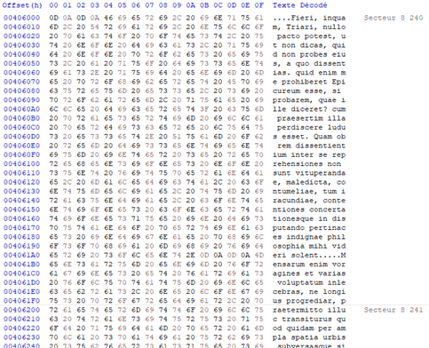
Since a cluster contains 8 sectors, we are confident that sectors 8240 to 8248 belong to the file we are reading. To know if the file continues after these 8 sectors, we have to go and see the value in the FAT for the cluster number we used. First you have to find the sector where the value is stored, then the offset in that sector.
FATOffset = N * 4
ThisFATSecNum = BPB_RsvdSecCnt + (FATOffset/BPB_BytsPerSec)
ThisFATEntOffset = FATOffset % BPB_BytsPerSec
With these formula, the calculated sector is 614 and the offset is 32.
Since the file system is FAT32, the values in the FAT are 32 bits (28 + 4 reserved). For FAT16, the values are 16 bits. To find out if our file is continuous, we need to read the 32-bit value at offset 32.
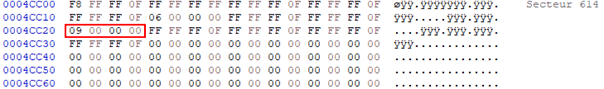
The highlighted value becomes our new cluster number. So we can find the first sector of the cluster, then read the 8 sectors and go back to the FAT to see if the file continues. If we redo the calculations, the sector remains the same, and the offset becomes 36. The 4 bytes at offset 36 have the value 0x0FFFFFFF, which indicates that the file does not continue further.
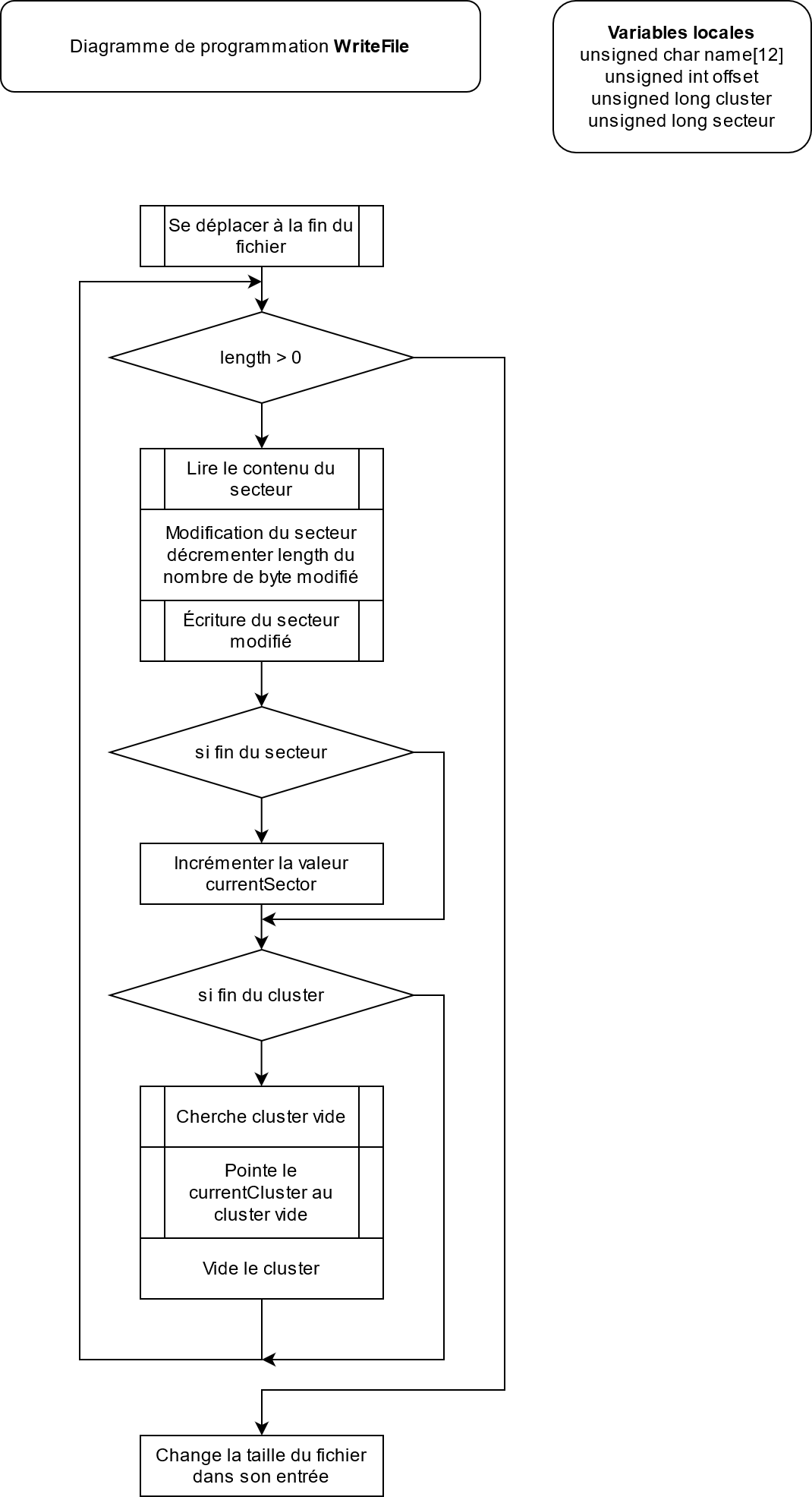
4.3.7. Writing a file
As with reading, the file must be opened with the OpenFile function before it can be written to. Once the file is open, it is possible to write information to an existing file. The only writing mode available is append mode. This means that the information will be added at the end of the file and nothing will be overwritten.
To write to a file, we must first read the sector we want to modify, modify it, and then write it back. The piece of code below does this.
// Read the sector
secteur = GetSectorFromCluster(bs, fi->currentCluster) + fi->currentSector;
SD_ReadBlock(TOKEN_RW, buf, bs->BytsPerSec, secteur);

for (x = (fi->Offset % 512); x < 512; x++)
{
		buf[x] = *texte++;
		fi->fileSize++;
		fi->Offset++;
		length--;
		if (length == 0) break;
}
// Write the changes
SD_WriteBlock(TOKEN_RW, buf, bs->BytsPerSec, secteur);
When writing to a file, it is very likely that a new cluster will need to be allocated for the file. The allocation can be summarised in 3 steps :
-
Search for an empty cluster in the FAT table.
-
Modify the old cluster to point to the new one.
-
Modify the new one to indicate the end of the file.
Note
When modifying the FAT table, it is important to modify ALL the tables. When reading the BootSector (Reading the BootSector), the value of BPB_NumFATs tells us how many tables are present.
4.4. E-Paper Display
4.4.1. What is the E-Paper technology
E-Paper is an electronically changeable display technology that seeks to mimic the appearance of paper. Like paper, this technology requires no energy to leave text on display. Unlike the screens we know, E-Papers do not have a backlight, they are reflective, meaning they use ambient light in the same way as conventional paper.
4.4.2. Why did I choose this technology ?
I chose this type of screen because it does not consume any energy as long as no changes are made. When reading a book, the pages remain static for some time before they refresh. This is why this type of screen is perfect for my project. It can also be noted that due to its low power consumption, there is no need to include an ON/OFF button, the project can remain powered constantly. It also has no backlighting, which makes it more pleasant to read than a conventional screen. The technology is quite slow, but this should not be a problem as when reading a book the screen does not need to be very responsive.
Advantages :
-
Low consumption.
-
Pleasant to read.
-
No backlight.
-
Text can remain displayed for long periods of time.
-
Very good display quality.
Disadvantages :
-
Low refresh rate.
-
High price.
-
Less supported compared to other technologies.
4.4.3. Functional principle
Each screen is composed of millions of capsules. These capsules contain negatively charged black pigments and positively charged white pigments in a transparent fluid. The capsules are placed between two electrodes that will allow to change the pigment’s position.
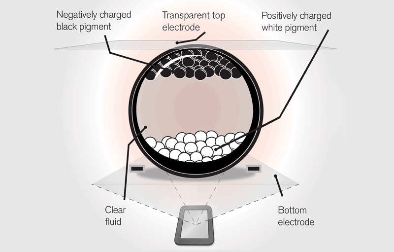
When a negative electric field is applied to the bottom electrode, the black pigments are pushed up and the white pigments are pulled down, changing the color of the pixel to black. If the electric field is positive, the opposite happens and the pixel becomes white. By performing this operation on the whole screen it is possible to display whatever you want.
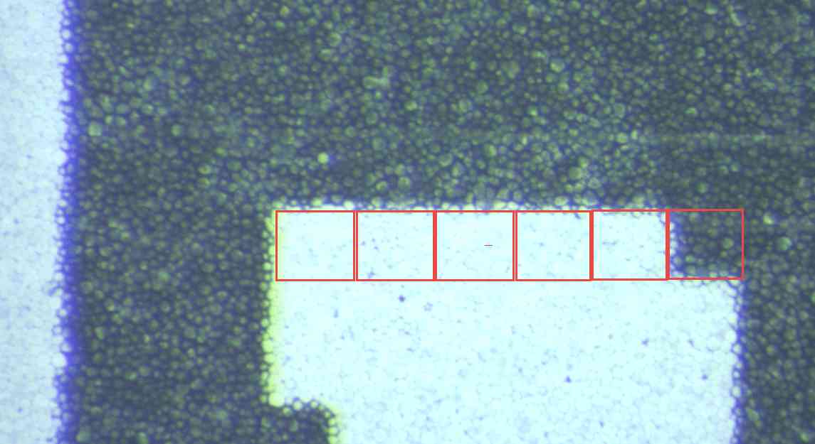
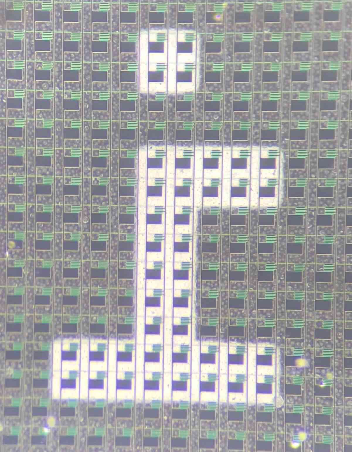
Each pixel contains several capsules, the Microscopic view of the capsules makes it possible to visualise the composition of a pixel in an E-Paper screen. One can easily visualize the many capsules in the black pixels. The red squares represent the size of 1 pixel.
I was also able to look at the back of my screen under a microscope. When you look at the screen from the back you can see the same display as on the front, but with reversed colours. This is because we are looking at the bottom of the capsule where the other pigments are located. Zooming in, we can also see the electrodes that control each pixel.
4.4.4. Communication
The microcontroller is not directly connected to the display, a driver is located between the two. This driver regulates the supply voltage. It also contains a level shifter to ensure that the I/O voltage is 3.3v.
The communication between the microcontroller and the display is an SPI communication (SPI bus) in which commands are sent. The commands can be sent with or without arguments. To communicate with the display I first wrote two functions allowing me to send information or commands
Functions to send a command or a single byte of information.
void EPD_SendData(unsigned char value)
{
	EPD_CS = 0;
	EPD_DC = EPD_DATA;

	SPI_SendByte(value);

	EPD_CS = 1;
}

void EPD_SendCommand(unsigned char cmd)
{
	EPD_CS = 0;
	EPD_DC = EPD_COMMAND;

	SPI_SendByte(cmd);

	EPD_CS = 1;
}
PIN |
Description |
VCC |
3.3 v |
GND |
GND |
DIN |
SPI MOSI |
CLK |
SPI CLK |
CS |
SPI Chip Select (active low) |
DC |
Data/Command control pin (High for data, and low for command) |
RST |
External reset pin (low for reset) |
BUSY |
Busy state output pin (low for busy) |
4.4.5. Display modes
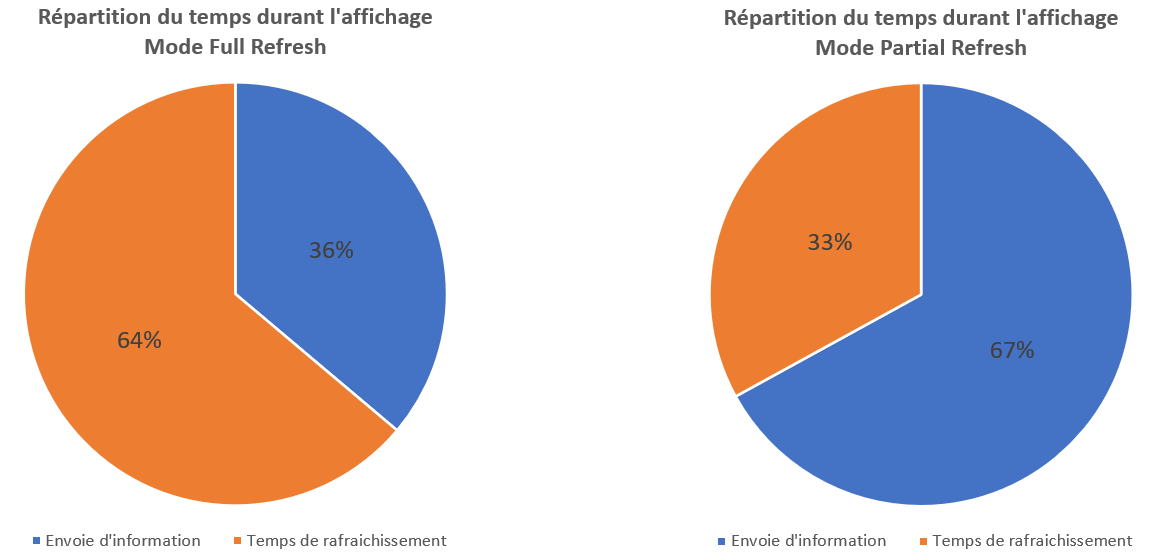
Some E-Papers have only one display mode, the screen used for the project has two. The first mode is the partial mode. It allows you to create a partial window on the screen and refresh only that part. This mode has a big speed advantage as the refresh time is 1.6 seconds. This is because only part of the screen is refreshed, so there is less information to send. This saves us from having to rewrite to the memory of the whole screen. The second mode is the full mode. In this mode it is mandatory to send ~64k of information because the screen buffer must be filled. It is therefore necessary to send (800/8) * 640 = 64000 bytes. That’s why its refresh time is longer since it is 4 seconds.
These times are already quite slow, but we must add the time it takes to send information to the screen. Two measurements with the logic analyser were carried out in order to measure the time necessary to display a page with a complete refresh and the time for a partial refresh.
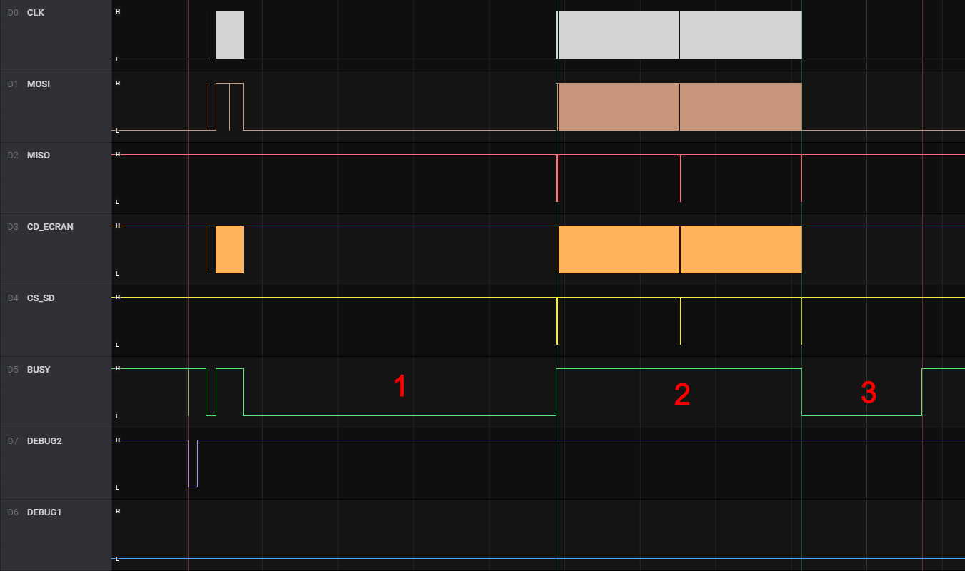
1 |
Full refresh time - 4.14s |
2 |
Sending information to the screen - 3.25s |
3 |
Partial refresh time - 1.60s |
The total time to display the information is 8.99 seconds. Unfortunately, it is not possible to send information during phase 1 because, according to the datasheet, no commands should be sent during the Busy period.
Note 1.5-4: This pin (BUSY_N) is BUSY_N state output pin. When BUSY_N is low, the operation of chip should not be interrupted and any commands should not be issued to the module. The driver IC will put BUSY_N pin low when the driver IC is working such as:
Outputting display waveform; or
Programmingwith OTP
Communicating with digital temperature sensor
— 7.5inch E-Paper V2 Specification waveshare
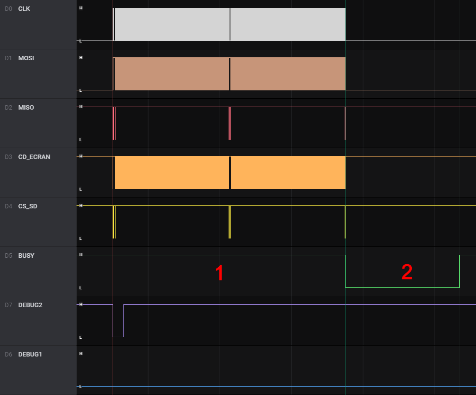
1 |
Sending information to the screen - 3.25s |
2 |
Partial refresh time - 1.60s |
The total time to display the information is 4.85 seconds.
4.4.6. Setting up the display
Once the library was tested, I started by reading the source code to understand how the screen worked. The source code of the library was very, if not too generic and it made it quite difficult to understand. So I decided to capture a frame with a logic analyser and then decode it by hand. This measurement allowed me to visualise the order of operations to initialise the screen, and to display text.
Once I understood how the screen operated, I was able to start developing functions on my microcontroller. The first functions allowed me to initialize the screen, then I added functions for the partial display. Finally, I developed the same functions I used in school (SelectPosCaractLiCo, AfficherCaractere, AfficherChaineAZT).
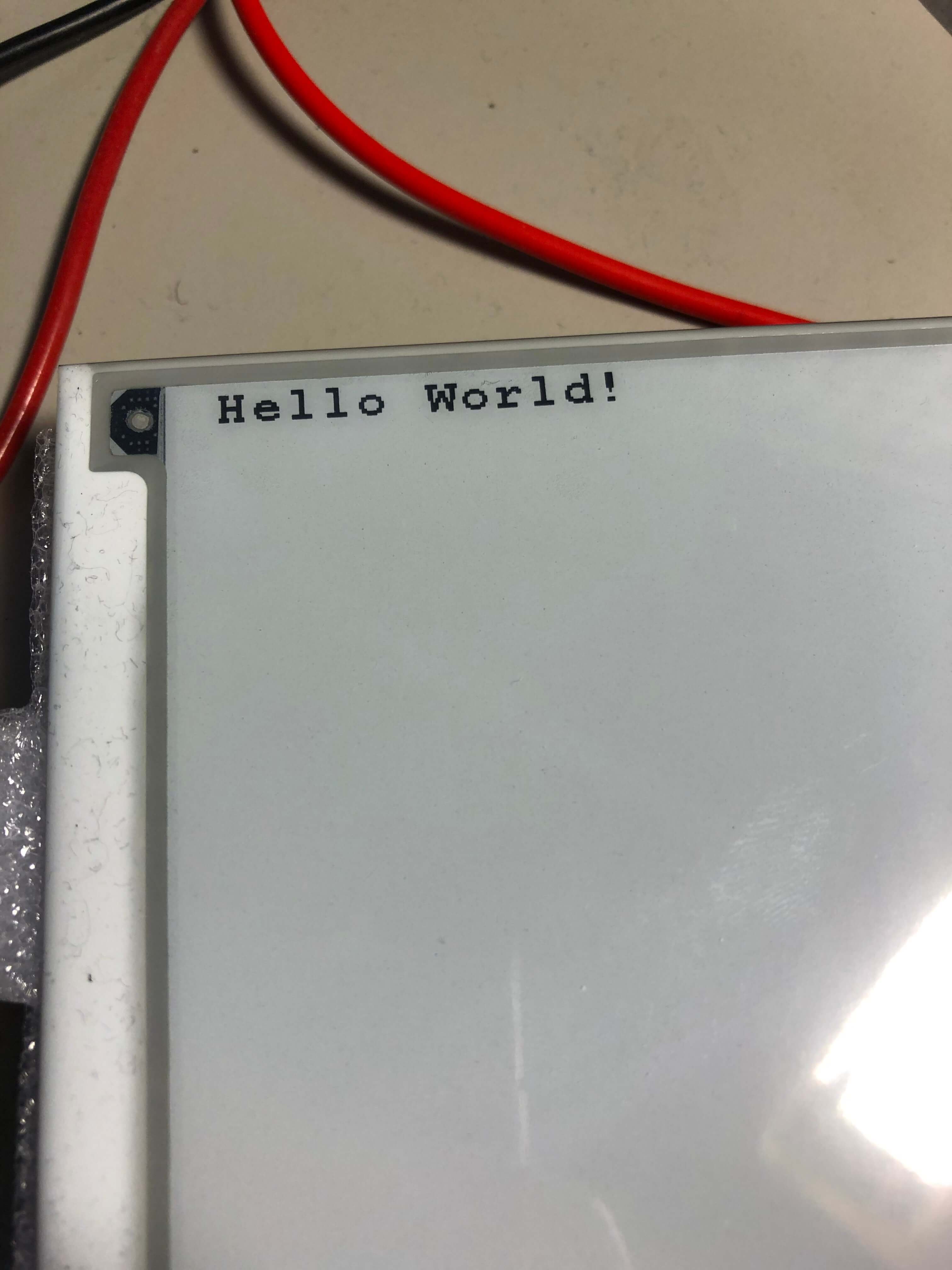
During my first tests, I simply displayed filled squares to make sure that the management of the partial mode was functional. I then retrieved an ASCII table from github, and started to display characters.
4.4.7. Problems encountered
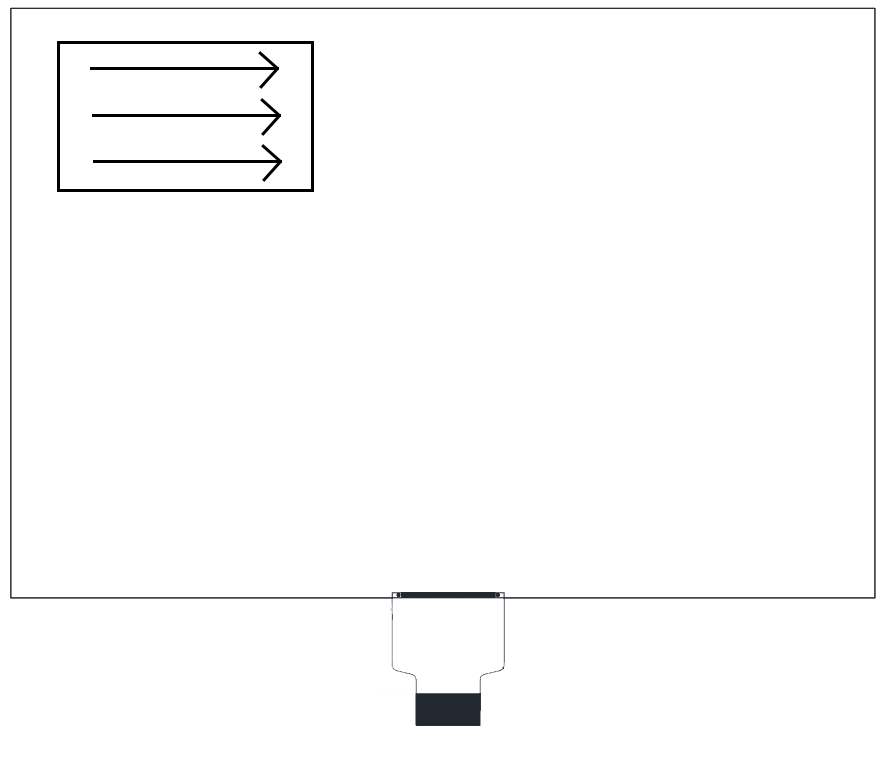
I have encountered a problem when using the ASCII table. While creating a partial region, the screen I am using fills the region starting at the top left and ending at the bottom right (landscape mode, see Byte order in a partial area). The table would have been perfectly functional if the screen had been used in landscape mode. However the books are displayed in portrait mode. So I had to make a function that would allow me to read each letter in the ASCII table vertically rather than horizontally so that they would be displayed in the correct direction.
I also had problems with the manufacturer’s library for the 7.5” screen not working. So I had to find another library that worked.
4.5. Interrupt 0 of the microcontroller
The external interrupt 0 of the microcontroller is activated when the RTC interrupt is triggered, or when the joystick is moved in a direction. I had to link all these signals to the same interrupt because the microcontroller has only 2 external interrupts (the PCA interrupts could potentially have been used). To make the interrupt active when one of the signals is active, I used an OR gate made with diodes.
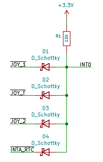
Warning
All signals must be active on the same value. The diodes have to be schottky diodes, a “classic” diode causes problems with level detection because of the 0.7v voltage drop.
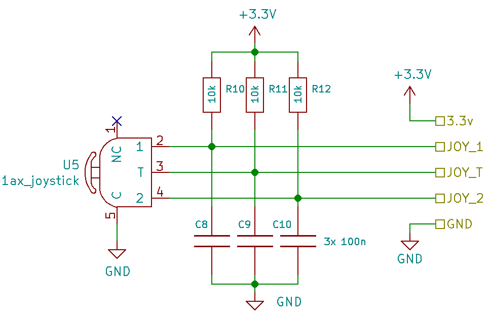
4.6. 1 axis joystick
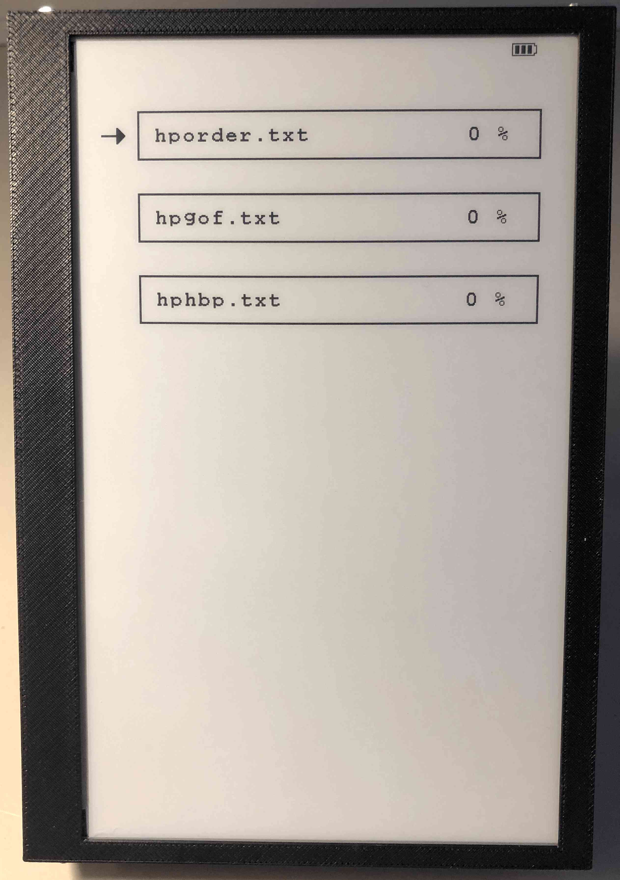
Thanks to the screen the books can be displayed, and the implementation of FAT32 allows me to read the files. Now I have to be able to choose the book to read, and turn the pages. At first I thought of using 3 push buttons ( forward, backward and selection), but I discovered the existence of 1 axis joysticks. This kind of joystick suits me perfectly, because it allows to go forward, backward and to select by pressing it.
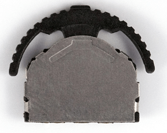
The model I use is made of 5 pins :
- C
- 1
- T
- 2
- Not connected
Pin C is a common pin to the other 3. When you apply 5v to pin C, and move the joystick, the pin 1, T or 2 will output 5v.
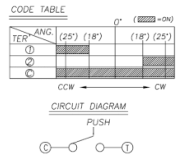
I chose to connect the common pin to ground so that a falling edge is generated. I also added capacitors to prevent rebounds.
4.7. Real Time Clock
E-Readers already exist on the market, so a datalogger was added to the project. This addition allows real magnitudes to be measured and then stored in a file on the microSD card. A RTC (Real Time Clock) was added to time-stamp and synchronise the measurements (every 10 minutes).
I chose to use a PCF85363A, because it allows to generate alarms and it has a small internal memory of 64 Bytes. The alarms allow to synchronize the measurements. In addition, the internal memory can be used in case writing to a file does not work or to store values if the microcontroller needs to be reset. Moreover, it consumes very little current, the datasheet indicates 10 uA. This RTC communicates via I2C (see I2C Bus).
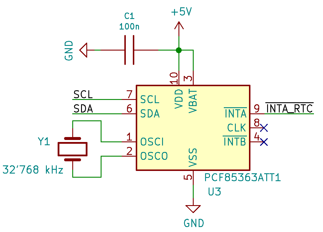
4.7.1. Interrupts configuration
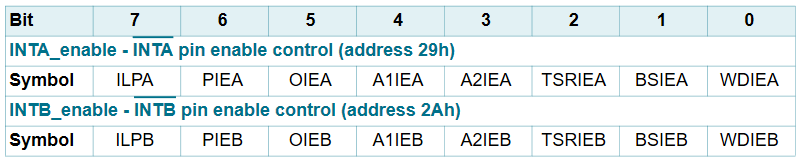
Since we want to synchronize the measurements every 10 minutes, we first have to configure the INTA output. The Pin_IO register is used to configure the outputs, the INTA pin is configured by INTAPM[1:0]. The value of INTAPM must be 0x02.

Secondly, the periodic interrupts must be configured. The two bits PI[1:0] are used to configure the interval between two periodic interrupts. By setting the PI value to 0x02, an interrupt will be generated every minute.

Finally, the INTA_enable register allows us to enable interrupt generation on the INTA pin. When the PIEA bit is set, periodic interrupts are generated on the INTA pin.
void RTC_ConfigInterrupt()
{
	unsigned char xdata _data[4];

	_data[0] = 0x27; // Address registre Pin_IO
	_data[1] = 0x82; // Configure the output /INTA
	_data[2] = 0x40; // Periodic interrupt once per minute
					// 0x40 -> once per minute
					// 0x20 -> once per second
	_data[3] = 0x40; // Periodic interrupt generated (INTA)

	I2CWrite (0, PCF85363_ADDR, _data, 4);
}
4.7.2. Time configuration
An example is given in the datasheet to set the time to 14 hours, 23 minutes and 19 seconds:
-
I2C START condition
-
I2C slave address + write (A2h)
-
register address (2Eh)
-
write data (set STOP, 01h)
-
write data (clear prescaler, A4h)
-
write data (100th seconds, 00h)
-
write data (Hours, 14h)
-
write data (Minutes, 23h)
-
write data (Seconds, 19h)
-
I2C START condition
-
I2C slave address + write (A2h)
-
register address (2Eh)
-
write data (clear STOP, 00h). Time starts counting from this point
-
I2C STOP condition
Note
It is possible to write to several consecutive registers at once because the register addresses are self-incrementing.
For time management a Time structure has been created. When setting
the time, the contents of the structure is sent to the memory of the
RTC.
typedef struct _time
{
	unsigned char seconde;  // 0..59
	unsigned char minute;   // 0..59
	unsigned char heure;    // 0..23
	unsigned char jour;     // 1..31
	unsigned char mois;     // 1..12
	unsigned char annee;    // 0..99 (2000 - 2099)
} Time;

void RTC_SetData(Time *time)
{
	unsigned char xdata _data[11];

	_data[0]  = PCF85363_REG_STOP;
	_data[1]  = 0x01; // Stop the clk
	_data[2]  = 0xA4; // Clear prescaler
	_data[3]  = 0x00; // 100th Sec
	_data[4]  = DecToBcd(time->seconde);
	_data[5]  = DecToBcd(time->minute);
	_data[6]  = DecToBcd(time->heure);
	_data[7]  = DecToBcd(time->jour);
	_data[8]  = 0; // Day of the week
	_data[9]  = DecToBcd(time->mois);
	_data[10] = DecToBcd(time->annee);

	I2CWrite(0, PCF85363_ADDR, _data, 11);
	I2CRegWrite(0, PCF85363_ADDR, PCF85363_REG_STOP, 0); // Restart the clock
}
4.7.3. Reading the time
Reading is easier than writing because there is no need to disable the clock. You only need to read the seconds register and the following 6.
Time RTC_ReadData()
{
	unsigned char xdata _data[7];
	Time xdata time;

	// Read the seconds register and the following 6
	I2CWrite(0, PCF85363_ADDR, PCF85363_REG_SEC, 1);
	I2CRead(0, PCF85363_ADDR, _data, 7);

	time.seconde = BcdToDec(_data[0] & 0x7F);
	time.minute  = BcdToDec(_data[1] & 0x7F);
	time.heure   = BcdToDec(_data[2] & 0x1F);
	time.jour    = BcdToDec(_data[3] & 0x3F);
	time.mois    = BcdToDec(_data[5] & 0x1F);
	time.annee   = BcdToDec(_data[6]);

	return time;
}
4.8. Datalogger
As mentioned before, a datalogger has been added to the project in order to measure real magnitudes. The project remains constantly powered thanks to its sleep mode, which reduces the consumption of the microcontroller, allowing measurements to be made all day long.
No sensors are included in the project, however a Grove connector allows multiple sensors to be connected which communicate via I2C (I2C Bus). The measurements are then added to the end of a text file present on the micro SD card (see Writing a file). If the card is not connected, the measurements are not made.
To test the datalogger, I used a development kit containing several ICs
such as a temperature sensor and an ADC. Every 10 minutes a temperature
reading and a voltage reading from the ADC is taken. The text below is
an example of what the datalogger writes to the log.txt file
annee.mois.jour;heure:minutes;temperature
2021.06.11;15:04;+29.56
2021.06.11;15:04;+29.56
2021.06.11;15:04;+29.62
2021.06.11;15:04;+29.56
2021.06.11;15:05;+29.62
2021.06.11;15:05;+29.68
2021.06.11;15:05;+29.68
2021.06.11;15:05;+29.56
2021.06.11;15:05;+29.62
2021.06.11;15:05;+29.56
2021.06.11;15:06;+29.62
Warning
No sensor should have the same address as the RTC (A2h)
A measurement with the logic analyzer allowed me to measure the time that the information takes to be read, then stored on the micro SD card. The time of the communication in I2C is 1ms, and the time of writing on the micro SD card is 19ms.
4.9. Battery
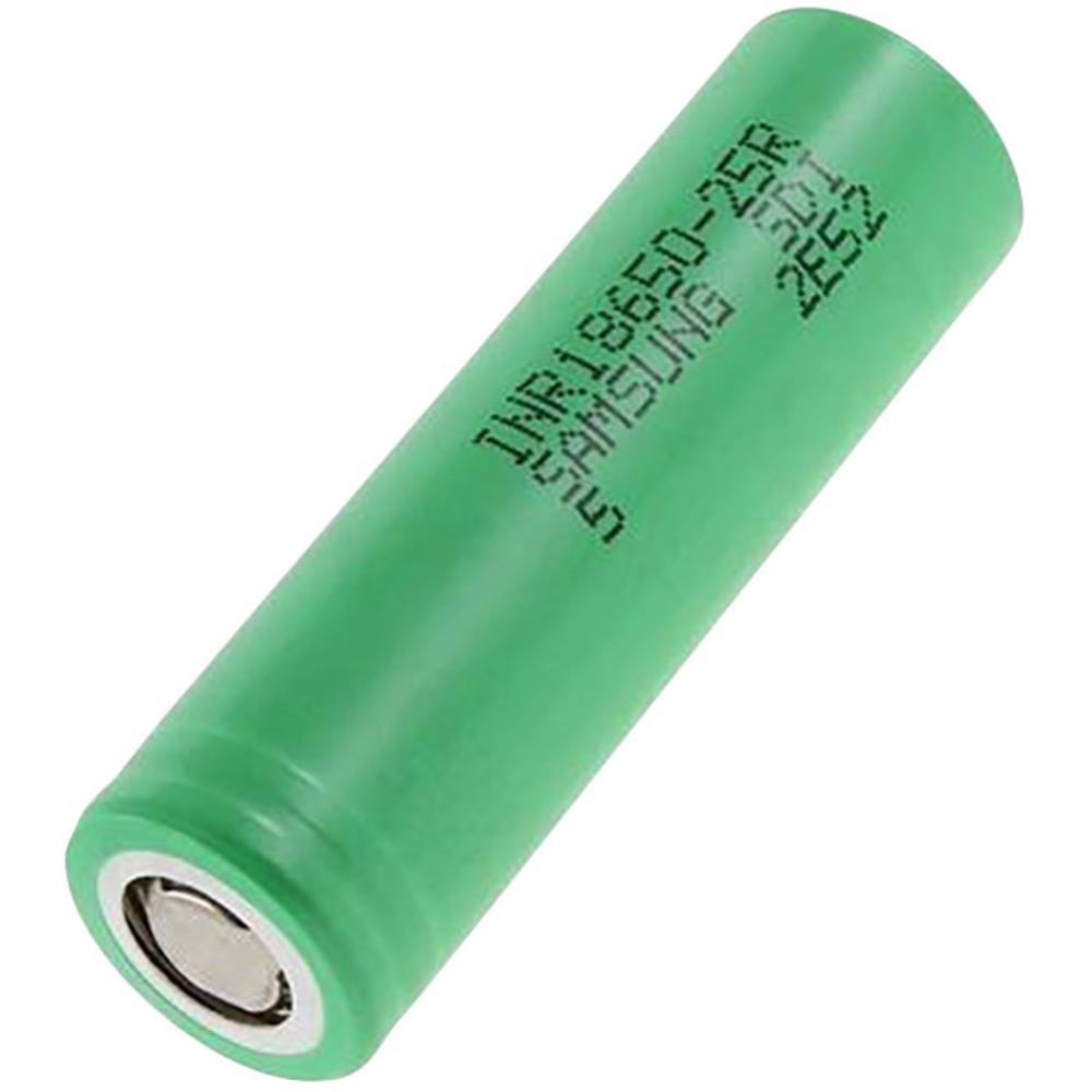
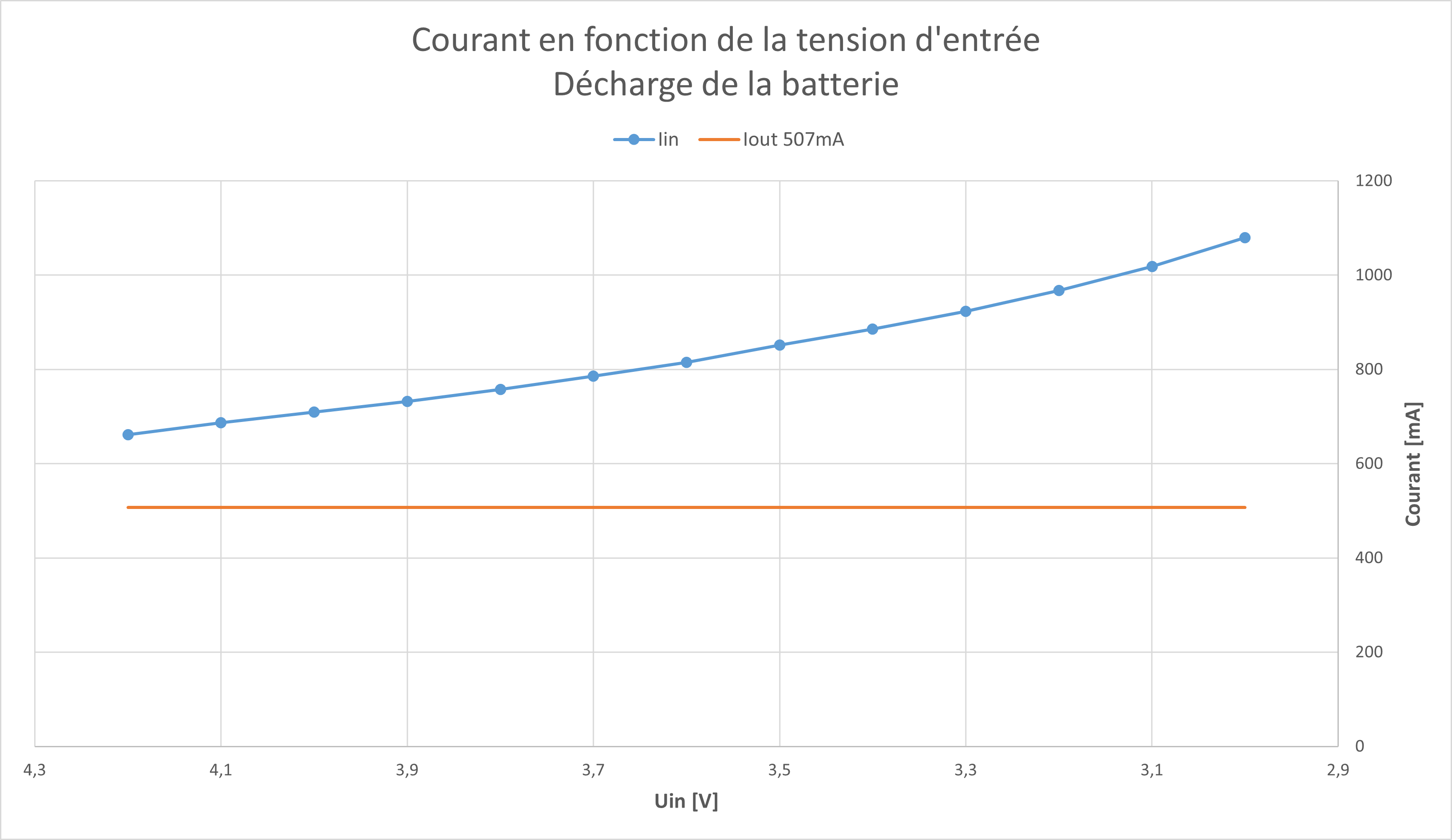
One of the constraints of the project is to be able to read a book from anywhere, so a battery is included. I tried to use a cylindrical Li-Ion battery. The capacity of the battery is ~3000mAh which allows the project to stay powered for a long time. However the battery does not have an over discharge protection. During a discharge measurement with an active load, I unfortunately discharged the battery too much.
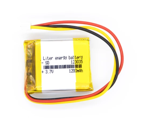
As a result, I had to change the battery and use a small LiPo battery with a capacity of only 1200mAh, which has protection against over charging and over discharging.
I was able to do a discharge measurement again using this new battery. The load was drawing a constant current of 500mA and the battery has a capacity of 1200mAh. In theory the discharge should last 2h24. The voltage measurements received from the active load does not seem to be correct (the discharge starts below 3.4v and ends around 1.8v) so the values will not be included in the report. However, the discharge time is 2h25, which corresponds well to the theoretical 2h24.
4.10. Charging the battery
To charge the battery, I used the USB LiIon/LiPoly charger - v1.2 from Adafruit. It allows to charge Lithium Ion and Lithium Polymer batteries. The module is powered by a USB Mini-B cable. A big advantage of the module is that the battery does not need to be disconnected from the circuit to charge. The fast charge current is 500mA, but this can be adjusted by changing a resistor on the module.
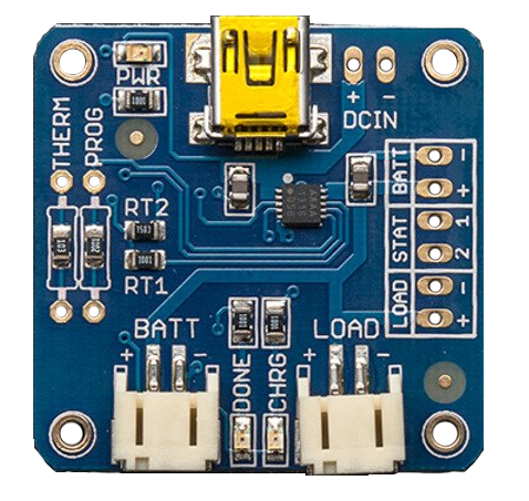
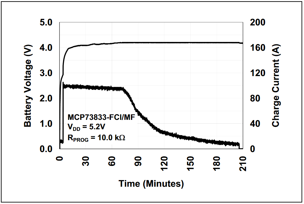
The module works in 3 stages which can be observed in the Complete charge cycle - Datasheet MCP73833 :
-
Preconditioning load
-
Fast constant current charging
-
Constant voltage trickle charge
The module also has two LEDs that serve as indicators. One LED indicates when the battery is being charged, and the other is lit when the battery has finished charging.
4.11. Regulation
The output voltage of the battery varies between 4.2 Volts and 3 Volts. I had to use a 5v Step-Up regulator. I chose to use the Adafruit MiniBoost 5V @ 1A - TPS61023 module from Adafruit because it has interesting characteristics. Its input voltage range is 2-5v, which corresponds to the output voltage of my battery. In addition, the module can draw up to 1 amp. My project will never reach 1A, or even come close, but this allows me to be sure that I will not be limited by the regulator.
4.11.1. Measurement sheet
Goal : Characterising an Adafruit module MiniBoost 5V @ 1A - TPS61023
Measurement schematic :
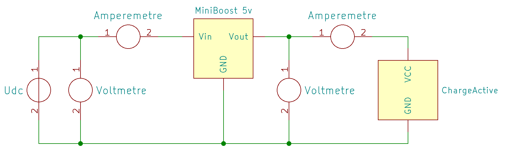
Measurements made :
Mesure 1 : Calculation of the minimum operating voltage according to the output current
Current [mA] |
Minimum tension [V] |
50 |
0.93 |
100 |
1.25 |
500 |
2.03 |
1000 |
2.91 |
To make this measurement, I drew a constant current through an active load, then reduced the supply voltage until the output voltage was no longer 5v.
Mesure 2 : Calculation of module efficiency
Uin [V] |
Uout [V] |
Iin [mA] |
Iout [mA] |
Pin [W] |
Pout [W] |
Efficiency [%] |
Theoretical efficiency [%] |
4.209 |
4.969 |
658.7 |
506.7 |
2.77 |
2.52 |
0.91 |
0.96 |
4.212 |
5.036 |
144.1 |
114.7 |
0.61 |
0.58 |
0.95 |
0.97 |
4.212 |
5.041 |
81.3 |
64.89 |
0.34 |
0.33 |
0.97 |
0.957 |
3.603 |
4.987 |
784 |
506.6 |
2.82 |
2.53 |
0.9 |
0.955 |
3.605 |
5.042 |
171 |
114.6 |
0.62 |
0.58 |
0.94 |
0.95 |
3.605 |
5.046 |
97.2 |
64.9 |
0.35 |
0.33 |
0.94 |
0.949 |
3.003 |
5.016 |
998.6 |
506.7 |
3 |
2.54 |
0.85 |
0.95 |
3.006 |
5.045 |
212.3 |
114.6 |
0.64 |
0.58 |
0.91 |
0.94 |
3.003 |
5.044 |
119.5 |
65 |
0.36 |
0.33 |
0.92 |
0.935 |
Theoretical efficiency corresponds to the measured efficiency.
Formula :
Pin = Uin * Iin = 4.209 * 658.7 * 10^-3 = 2.77 [W]
Pout = Uout * Iout = 4.969 * 506.7 * 10^-3 = 2.52 [W]
Rendement = Pout / Pin = 2.52 / 2.77 = 91 [%]
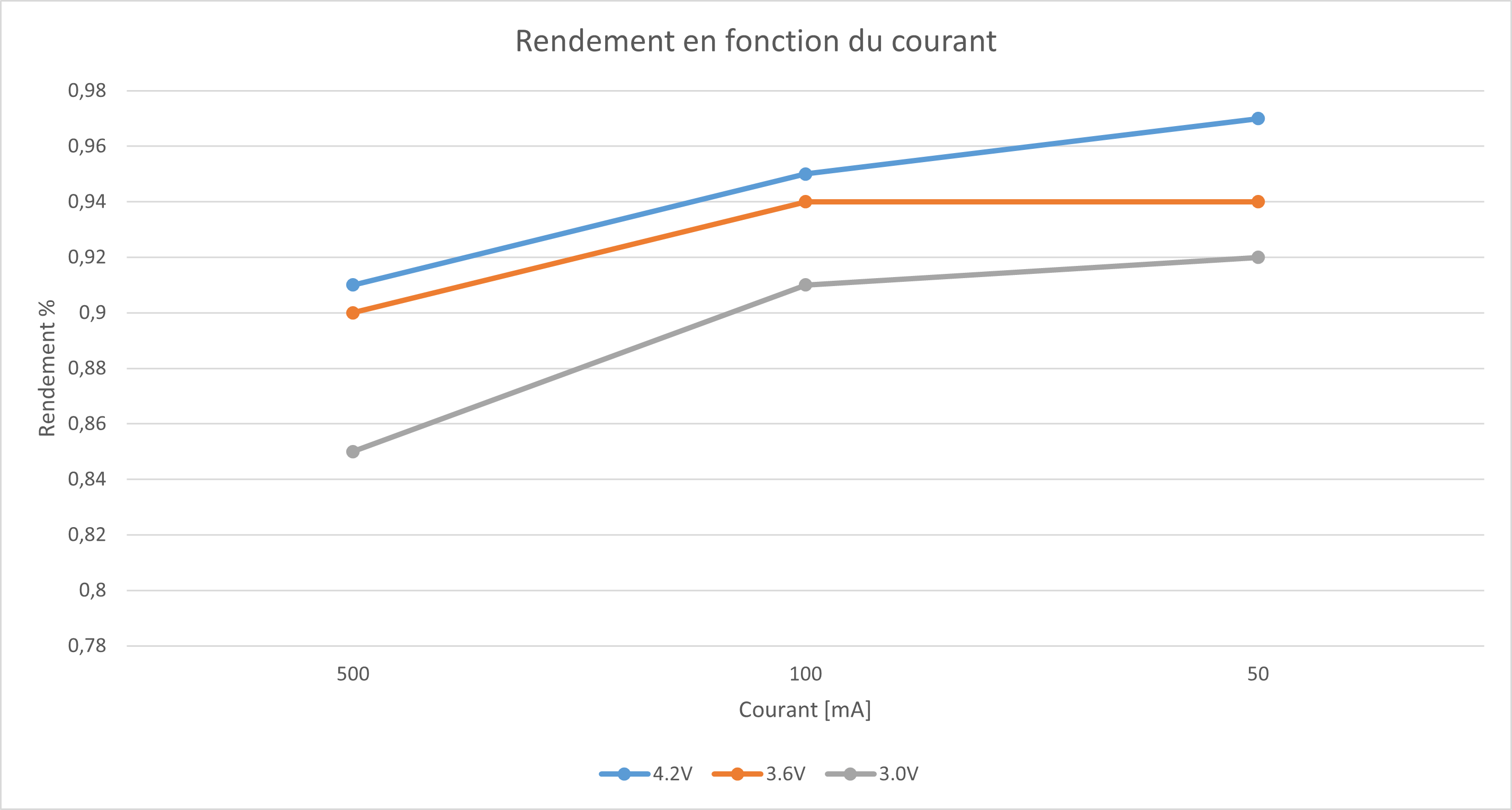
Conclusion : It can be seen that the efficiency is better when the input voltage is high and the output current is low.
Mesure 3 : Calculation of the power dissipated by the circuit for a 50 mA, 100 mA and 500 mA load
Vin = 4.2v
Power dissipation for 50 [mA] : Pdissipated = Pin - Pout = 0.34 - 0.33 = 10 [mW]
Power dissipation for 100 [mA] : Pdissipated = 0.62 - 0.58 = 40 [mW]
Power dissipation for 500 [mA] : Pdissipated = 2.77 - 2.52 = 250 [mW]
Vin = 3.6v
Power dissipation for 50 [mA] : Pdissipated = 0.35 - 0.33 = 20 [mW]
Power dissipation for 100 [mA] : Pdissipated = 0.62 - 0.58 = 40 [mW]
Power dissipation for 500 [mA] : Pdissipated = 2.82 - 2.53 = 290 [mW]
Vin = 3.0v
Power dissipation for 50 [mA] : Pdissipated = 0.36 - 0.33 = 30 [mW]
Power dissipation for 100 [mA] : Pdissipated = 0.64 - 0.58 = 60 [mW]
Power dissipation for 500 [mA] : Pdissipated = 3.00 - 2.54 = 460 [mW]
Mesure 4 : Measuring the input current as a function of the input voltage
This was done by drawing a constant current. I then measured the input current as a function of the battery voltage (in discharge).
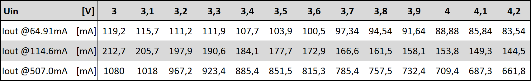
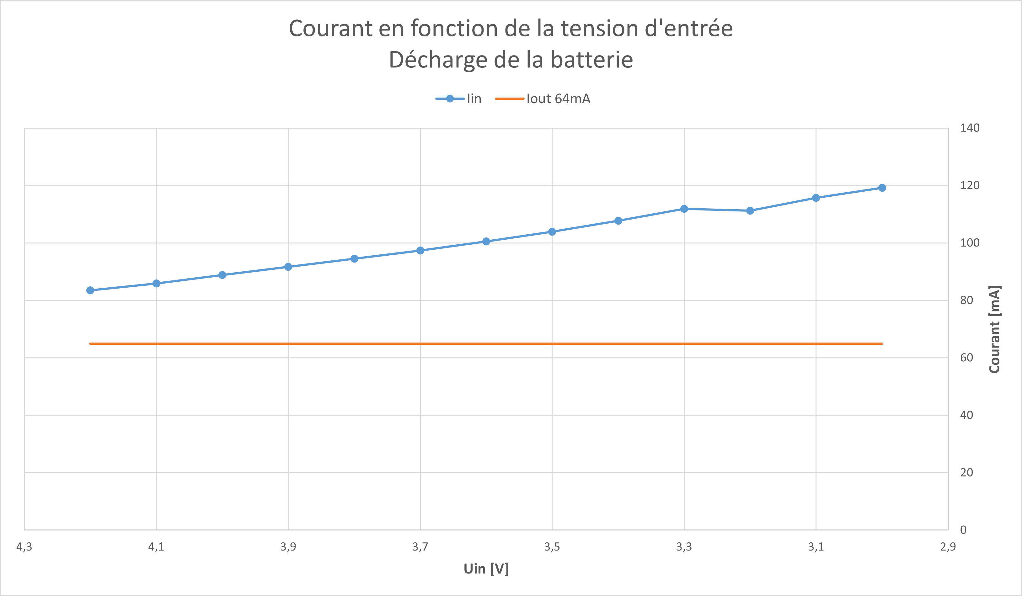
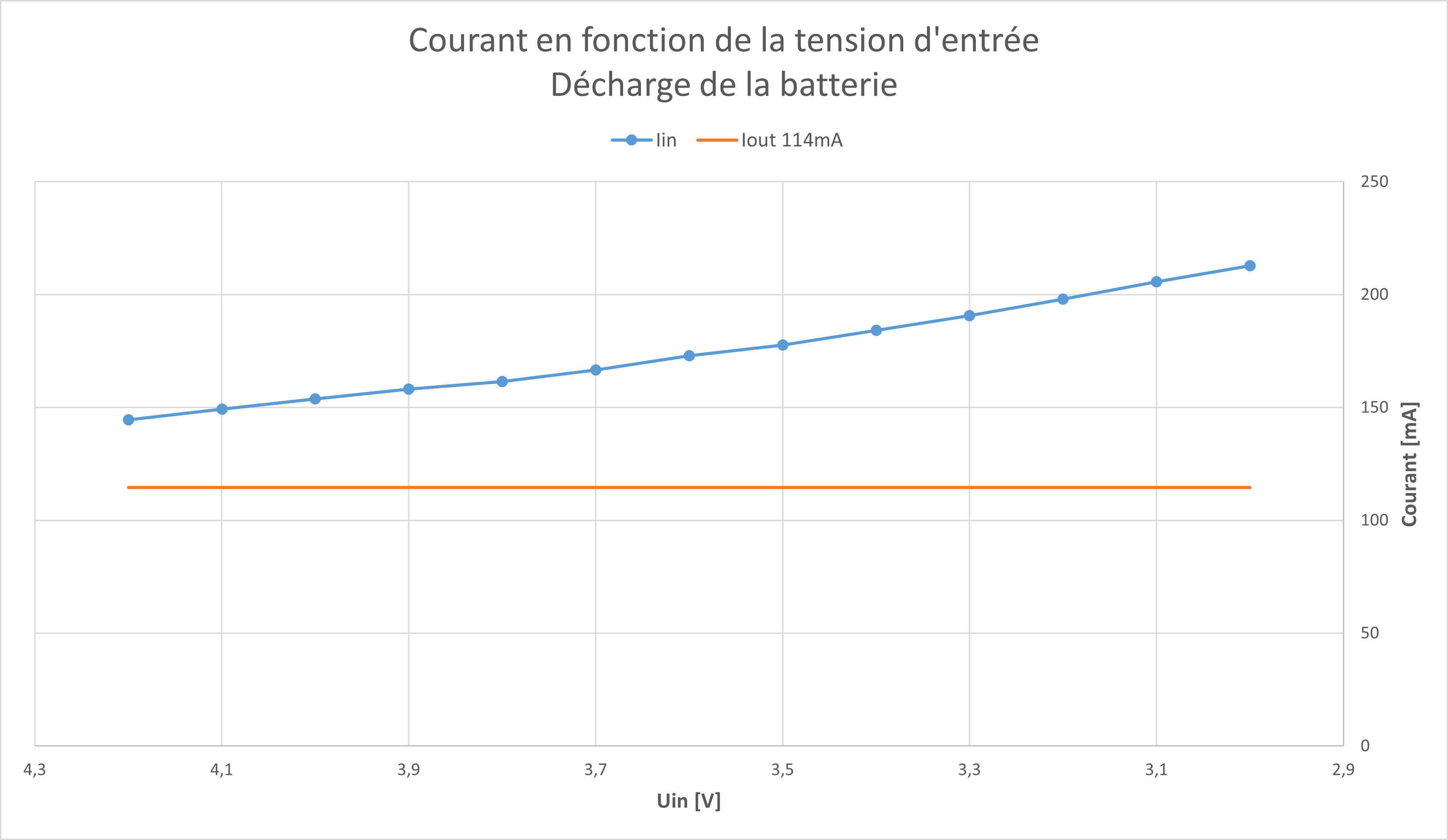
Conclusion : As we saw in measure 2, the lower the battery voltage, the lower the efficiency.
4.12. Consumption
Since one of the constraints of this project is low current consumption, I had to find a way to limit the power consumption of the microcontroller when it is not used. To do this, I found two possibilities. The first would be to completely shut down the MCU and its internal controllers. This method consumes about 1 [uA] (theoretical value), however to get out of this mode a reset of the microcontroller must be done. The second method would be to switch from the high frequency internal oscillator (configured at 48 MHz) to the low frequency internal oscillator with a frequency of 10 kHz.
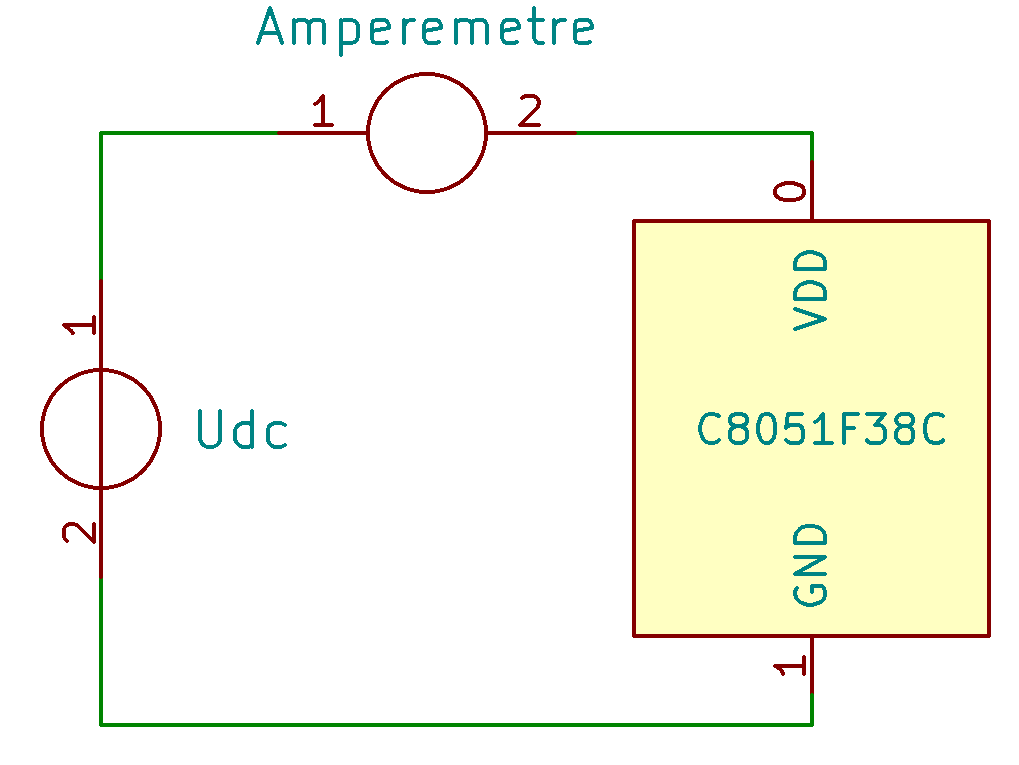
4.12.1. Measurement sheet
Goal : Measure the power consumption of the microcontroller configured in different modes
Setting up the measure : In order to get more accurate results, I decided to desolder the R4 resistor from the microcontroller board so that I would not have to subtract the LED current.
Mesure 1 : Consumption of the microcontroller powered directly by a lab power supply
Theoretical values
Datasheet page 42 (Table 5.2. Global Electrical Characteristics)
SYSCLK |
Parameter |
Consumption (mA) |
48 MHz |
- |
14.0 |
48 MHz |
IDLE MODE |
8.0 |
48 MHz |
STOP MODE |
0.001 |
80 kHz |
- |
0.280 |
80 kHz |
IDLE MODE |
0.220 |
80 kHz |
STOP MODE |
0.001 |
Note
Theoretical values with the lowest SYSCLK are 80 kHz. Comparisons will be made with a 10 kHz SYSCLK.
Measurement schematic
Result of the measure
48 MHz
REG0 |
REG1 |
Mode |
Current consumed |
ON |
ON |
Normal |
14.13 [mA] |
ON |
ON |
IDLE |
8.521 [mA] |
OFF |
OFF |
STOP |
1 [uA] |
10 kHz
REG0 |
REG1 |
Mode |
Current consumed |
ON |
ON |
Normal |
251 [uA] |
ON |
ON |
IDLE |
251 [uA] |
LOW |
LOW |
Normal |
147 [uA] |
OFF |
OFF |
STOP |
1 [uA] |
Notes on the measure : STOP Mode is the best way to reduce power consumption, however to restart the microcontroller it must be reset, which can be problematic. The second best option would be to switch both internal controllers to low power mode and use the internal low frequency oscillator at 10 kHz.
According to my measurements, IDLE mode has no impact on power consumption when the microcontroller uses the internal clock at 10 kHz. However, using the controllers in low power mode reduces the power consumption by 100 [uA].
Conclusion : The measured values correspond well to the values found in the datasheet. The STOP mode would consume about 14000x less current. By changing the frequency, it would be possible to reduce the consumption by almost 100x.
Choosen mode :
Mode Active |
48 MHz, Regulators ON, Mode normal |
Mode Sleep |
10 kHz, Regulators Low, Mode normal |
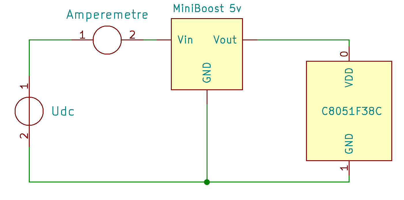
Mesure 2 : Power consumption of the microcontroller powered by a DC/DC converter
Information on the measure : Vbat represents the voltage range of the battery, in the measurements these voltages were simulated by a lab supply
Mesure schematic
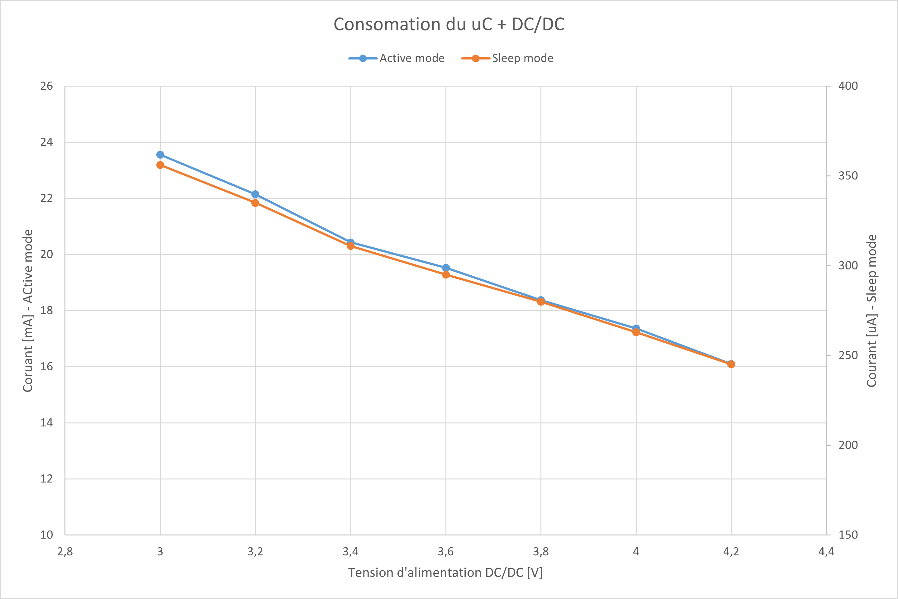
Result of the measure
Vbat [V] |
Active [mA] |
Sleep [uA] |
4.2 |
16.09 |
245 |
4 |
17.36 |
263 |
3.8 |
18.37 |
280 |
3.6 |
19.53 |
295 |
3.4 |
20.43 |
311 |
3.2 |
22.15 |
335 |
3 |
23.56 |
356 |
When the battery level is low, the power consumption of the microcontroller increases by 45% (difference between 4.2v and 3v).
4.12.2. Total consumption
The power consumption of the microcontroller has been reduced, but I did not take into account the power consumption of the other modules on the motherboard. In Sleep mode, the motherboard consumes 2.4mA. With a 1200mAh battery, the project can stay powered for 500 hours. Of the 2.4mA, 1.24mA is consumed by the micro SD card module, 810uA is consumed by the display driver, and about 350uA by the microcontroller.
In Active mode with a Vbat voltage of 3v, and refreshing the screen, peaks of 50mA can be observed, but the average is around 35mA (3v is when the DC/DC converter consumes the most, so the worst case).
4.13. PCB
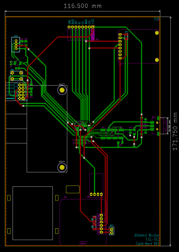
During the this project, I had the opportunity to produce 4 PCBs (Printed Circuit Boards). Two were produced in order to have a modular approach. If one of the two designs did not work, it would not have prevented the motherboard from working. It would simply have to be modified and rebuilt. The first module produced contains a 1 axis joystick (1 axis joystick). The second module contains an RTC and its quartz (Real Time Clock). The two other pcb’s are motherboards. The first one allows to group all the modules and has pins to make measurements. The second motherboard is the final version, it has all the components directly on the pcb (except purchased modules).
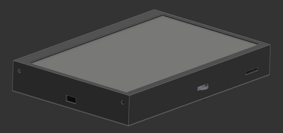
4.14. Case
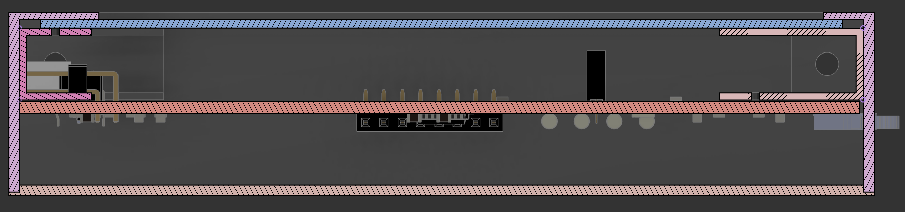
To make the project more beautiful and easier to carry, I made a case that will later be 3D printed. The Cross-section of the case is a cutaway view from the bottom of the case. You can see, in blue, the E-Paper screen which is stuck against the front of the case and is supported by 4 brackets screwed to the case. Two of these brackets are used to hold the PCB which can be seen in orange. Finally the last piece is the back of the case.
5. Chronological summary of development
The first week was mainly dedicated to the analysis of the project. During this period I looked for the components I wanted to use. First of all, I looked for modules for battery charging (battery charger and DC/DC converter). I then looked for an RTC in order to time-stamp the measurements that will be made by connecting a board containing several I2C modules such as a temperature sensor and an ADC. During this week I also looked at the power consumption of the microcontroller and the possibility of entering a deep sleep mode. I then listed all the tasks in order to realize my planning. I also made the first version of my block diagram, the FAST diagram and the synoptic diagram in order to have a global view of the project. Towards the end of the week, I started the conception of the file converter, then I tested the presence detection for the micro SD card.
The first two days of the second week were devoted to FAT32. I took the functions I had developed previously and modified the code to make it cleaner. I also wrote new functions such as OpenFile, ReadFile, FileSeek. These functions allowed me to easily interact with the files on the micro SD card. I then wanted to work on the management of the E-Paper screen, but I had not yet received it. So I decided to test the power reduction of the microcontroller. I was able to find out more about the different modes offered by the microcontroller, and I tested the different modes to see if they were usable or not. Around the middle/end of the week I received the E-Paper screen. So I stopped the power measurements to test the screen with libraries, and then I tried to understand how it worked.
The third week was mainly devoted to the screen. I continued to explore the screen with measurements made with a logic analyser. I spent a little time on the file converter to add a signature to the converted files. This signature will allow me later to filter the lambda files from the files that are converted books. After discovering the screen and how it works, I started writing functions on the microcontroller (C8051F381) to control the screen. After writing these functions, I started writing functions to display text, and by the end of the week I could display a page of text from a book stored on the micro SD card.
On Monday of the fourth week, I finished the functions to display a book by saving the reading progress in the file header. I finished testing the different modes of the microcontroller. I then wanted to test the battery charging module and the 5v DC/DC converter. Unfortunately during the test, the charger got fried and the DC/DC converter was not working either. So I changed the task, and started to make the wiring diagrams of the RTC module, as well as the joystick module. Once the two electrical schematics were finished, I made pcb’s. The purpose of these two prototypes was to have a mini module that connects to the motherboard in order to test them separately before including them in the final pcb.
The fifth week started with the realization of the pcb for the motherboard. The aim of this board was to have a very modular approach in order to troubleshoot only one module in case of a problem. I then received the two pcb’s that had been made the previous week, I was then able to assemble and test them. The pcb with the joystick worked well, I had the opportunity to measure the bounces with the oscilloscope. I did not test the RTC module immediately after mounting it, I tested it later in the week and it worked fine. During this week I received a new battery charger and a new DC/DC converter. I was able to measure the discharge of the battery with an active load during the week. After checking the measurements, they were not correct. On the last day of the week I was able to characterise the DC/DC converter.
The beginning of the sixth week was used to make the final pcb. Since all the components were tested on the prototype motherboard, I was sure that I could make the final pcb. I then started to design a menu to display the available books. I also set up the menu navigation and book selection. At the end of the week, I made functions for the RTC and time and alarm management.
The seventh week started with the implementation of the WriteFile function. I had to do some research to find out if there were any constraints when writing to a file. Once I found the information, I started programming. Once the writing was functional, I needed a sensor to test the datalogger. I set up a temperature sensor and then put together all the necessary components to make the datalogger work. The rest of the activities during the week were mainly bug solving and making a case.
The last week was mainly devoted to writing the report and fixing bugs.
6. Conclusion
6.1. Technical aspects of the project
Several improvements can be considered. The first would be to add a configuration menu that would allow you to modify the size of the text, or to configure the time between each measurement. Another possible improvement would be to add fonts on the SD card.
In my opinion, one of the best possible improvements would be to change the way the converter works. Instead of extracting the text, an image should be generated and then displayed on the E-Paper screen. This change would make it possible to display images and read more technical books that contain diagrams and images rather than just text.
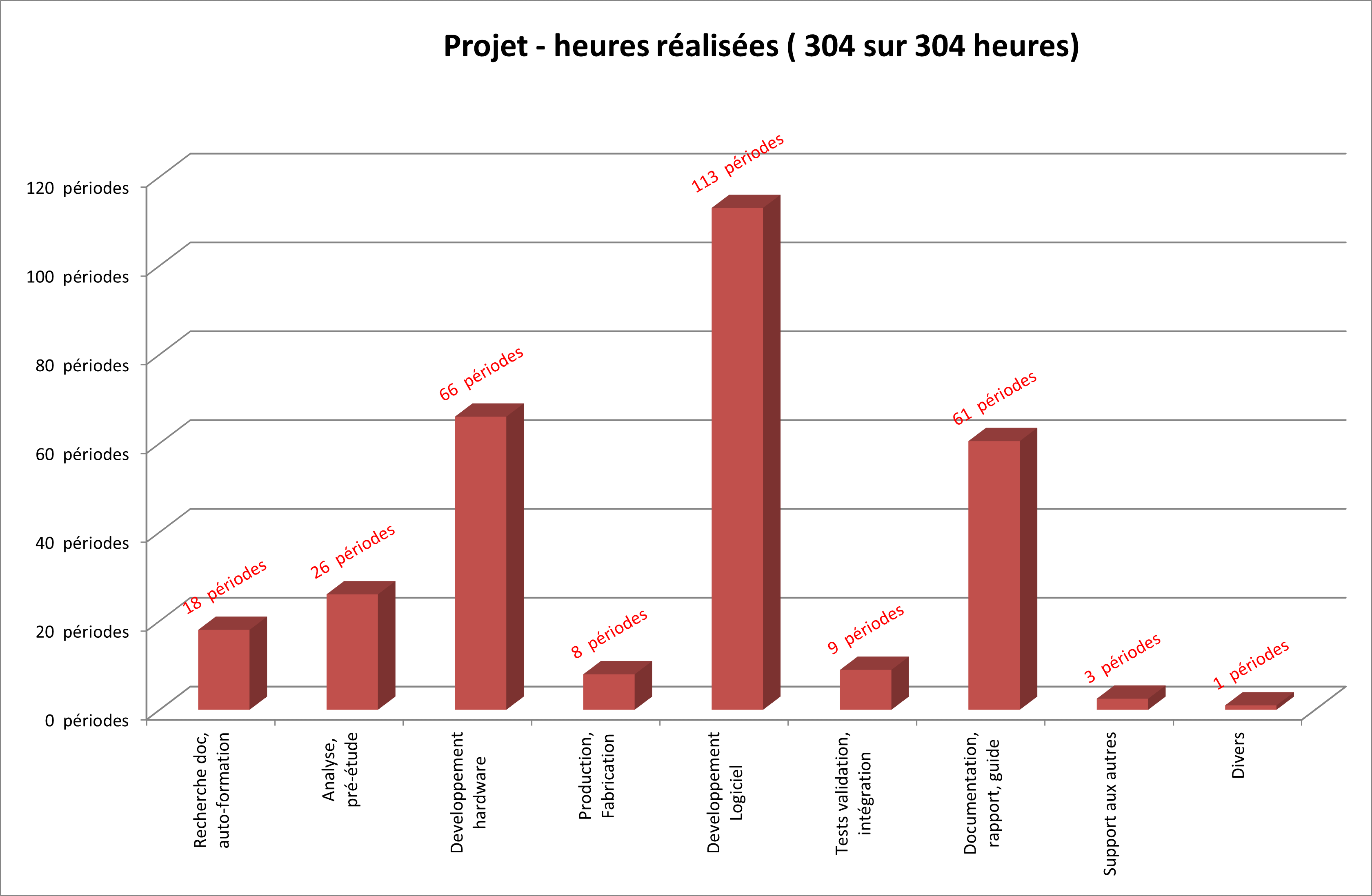
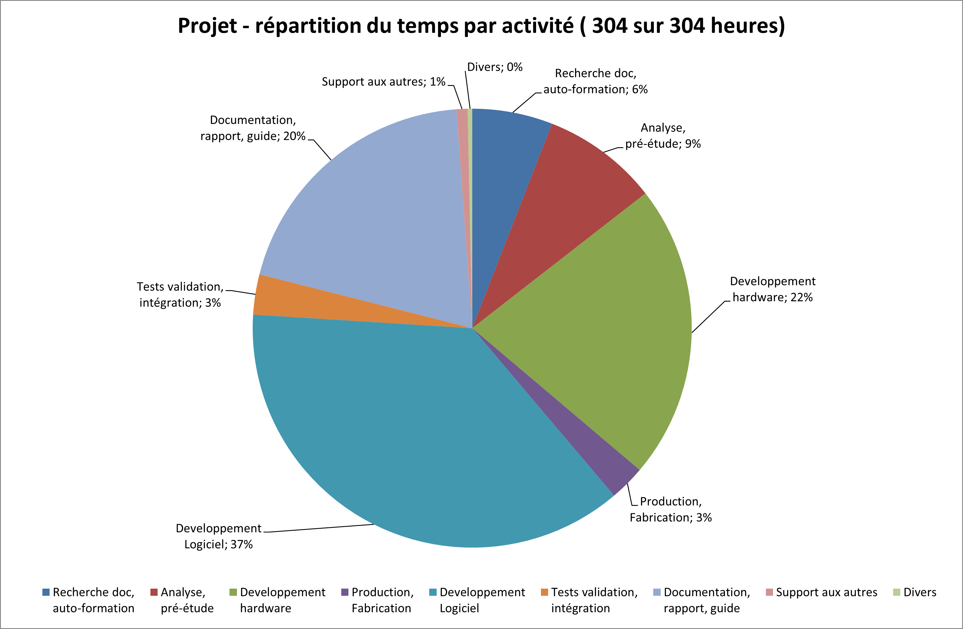
6.2. Project management
7. Development tools used
Logiciel |
Révision / Version |
Utilisation |
Keil uVision 5 |
5.27.1.0 |
programming the MCU |
KiCad |
5.1.7 |
Electric schematic + PCB |
Python |
3.8.5 |
Application development |
Excel |
2105 |
Project management, graph |
asciidoctor |
1.5.4 |
Report redaction |
8. Bibliographie
SD Card
http://www.chlazza.net/sdcardinfo.html
http://www.dejazzer.com/ee379/lecture_notes/lec12_sd_card.pdf
FAT32
https://www.win.tue.nl/~aeb/linux/fs/fat/fatgen103.pdf
http://www.cs.uni.edu/~diesburg/courses/cop4610_fall10/week11/week11.pdf
http://www.cs.uni.edu/~diesburg/courses/cop4610_fall10/week12/week12.pdf
E-Paper display
https://www.waveshare.com/w/upload/6/60/7.5inch_e-Paper_V2_Specification.pdf
https://www.waveshare.com/7.5inch-e-Paper.htm
https://www.reddit.com/r/arduino/comments/jkg3vv/need_help_with_waveshare_epaper/
https://v4.cecdn.yun300.cn/100001_1909185148/GD7965.pdf
https://www.visionect.com/blog/electronic-paper-explained-what-is-it-and-how-does-it-work/
https://github.com/avirtuos/waveshare/tree/master/tutorials/demo/stm32/Fonts
RTC
https://www.nxp.com/docs/en/data-sheet/PCF85063A.pdf
https://www.digikey.ch/product-detail/fr/nxp-usa-inc/PCF85363ATT-AJ/568-12408-2-ND/5170044
https://www.digikey.ch/product-detail/fr/micro-crystal-ag/CM8V-T1A-32-768KHZ-9PF-20PPM-TA-QC/2195-CM8V-T1A-32-768KHZ-9PF-20PPM-TA-QCCT-ND/10500166
Joystick
https://cdn.sparkfun.com/datasheets/Components/Switches/LEVER8184.pdf
Battery
https://www.distrelec.ch/Web/Downloads/_t/ds/PIS-1135_eng_tds.pdf
Battery charger
https://www.adafruit.com/product/4410
https://www.adafruit.com/product/259
https://forums.adafruit.com/viewtopic.php?f=8&p=727281
https://cdn-shop.adafruit.com/datasheets/MCP73833.pdf
DC/DC converter
https://www.digikey.ch/product-detail/fr/adafruit-industries-llc/3661/1528-2445-ND/7915572
https://www.adafruit.com/product/4654